

Photonic crystals in biology
Photonic crystals in biology
Photonic crystals in biology

Create successful ePaper yourself
Turn your PDF publications into a flip-book with our unique Google optimized e-Paper software.
Poster Session, Tuesday, June 15<br />
Theme A1 - B702<br />
The Hydrogen Sens<strong>in</strong>g Properties of Pd Nanowires<br />
ennik 1 *, Necmett<strong>in</strong> K 1 and Zafer Ziya Öztürk 1, 2<br />
1 Gebze Institute of Technology, Science Faculty, Department of Physics, Kocaeli 41400, Turkey<br />
2 TUBITAK Marmara Research Centre, P.O. Box 21, 41470 Gebze Kocaeli, Turkey<br />
Abstract- In this study, Pd nanowires are successfully fabricated directly on Highly Oriented Pyrolytic Graphite (HOPG) depend<strong>in</strong>g on time<br />
us<strong>in</strong>g palladium nitrate solution at room temperature and then the hydrogen sens<strong>in</strong>g properties of the fabricated these structures are <strong>in</strong>vestigated<br />
<strong>in</strong> the various concentrations of H 2 . Nanowires with diameters approximately 100 nm are obta<strong>in</strong>ed by electrodeposition onto the step edges on<br />
the surface of a ZYH quality of HOPG. The sensitivity is observed approximately 2 % for 1000 ppm H2 at room temperature.<br />
Hydrogen has numerous applications <strong>in</strong> <strong>in</strong>dustry, such as<br />
chemical production, fuel cell technology, and rocket eng<strong>in</strong>es<br />
[1]. However, the flammable and explosive properties of<br />
hydrogen gas make its detection an important issue [2]. That’s<br />
why nanotechnology has been used and become more vogues<br />
day by day. Nanostructures such as nanotubes [3] and<br />
nanowires [4] have been fabricated for H 2 gas sens<strong>in</strong>g.<br />
Pd plat<strong>in</strong>g solutions were used: aqueous 2 mM Pd(NO3) 2 ,<br />
0.1 M HClO 4 . These solutions were prepared us<strong>in</strong>g nanopure<br />
water (r ~ <br />
experiment. The surface of highly oriented pyrolytic graphite<br />
(HOPG) crystal was cleaved us<strong>in</strong>g adhesive tape immediately<br />
prior to use. The growth of metal nanowires was carried out<br />
us<strong>in</strong>g the 3 - pulse potential program.<br />
The values for the oxidation potential, E<br />
ox<br />
, the nucleation<br />
potential, E nuc<br />
, and the growth potential, E grow<br />
are 0.8 V, -<br />
0.8 V and 0.3 V, respectively. The oxidation potential was 5 s<br />
for activat<strong>in</strong>g the electrodeposition. The nucleation potential<br />
was chosen for 0.01 s and this potential determ<strong>in</strong>ed the<br />
form<strong>in</strong>g of nanowires through growth potential and growth<br />
time that are called deposition potential and deposition time,<br />
respectively. Follow<strong>in</strong>g deposition, the graphite was removed<br />
from the plat<strong>in</strong>g solution, r<strong>in</strong>sed with water, and air dried prior<br />
to characterization us<strong>in</strong>g SEM.<br />
sensor were purged with 200 sccm high purity N 2 . As shown<br />
<strong>in</strong> Figure 2, the resistance of the sensor was <strong>in</strong>creased by the<br />
<strong>in</strong>creas<strong>in</strong>g concentrations of H 2 .<br />
Figure 2. The resistance versus the concentrations of hydrogen for the<br />
Pd nanowire sensor [4]<br />
In conclusion, electrochemical step edge decoration (ESED)<br />
is very general method for prepar<strong>in</strong>g nanowires that are size<br />
and shape uniformity. Pd nanowires fabricated on HOPG were<br />
used as H 2 gas sensor. The results of gas sens<strong>in</strong>g<br />
measurements have shown that Pd nanowires sensor is<br />
abundant at room temperature.<br />
This work was supported by TUBITAK under Grant No.<br />
TBAG106T546.<br />
*Correspond<strong>in</strong>g author: zozturk@gyte.edu.tr<br />
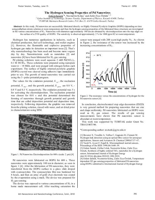
Figure 1. Pd Nanowires Electrodeposition for 600 s (scale: 2 [4]<br />
Pd nanowires were fabricated on HOPG for 600 s. These<br />
nanowires were approximately 100 nm <strong>in</strong> diameter, as seen <strong>in</strong><br />
figure 1 [4]. After the fabrication of Pd nanowires, they were<br />
transferred fro m the HOPG surface to a glass slide droped<br />
with cyanoacrylate. The cyanoacrylate film was hardened for<br />
8 hours, and then an array of gold (Au) electrode was coated<br />
by the evaporation us<strong>in</strong>g a mask. The device was prepared for<br />
H 2The gas sens<strong>in</strong>g.<br />
device was exposed to various concentrations of H 2 <strong>in</strong> a<br />
home made measurement cell. After reach<strong>in</strong>g saturation the<br />
[1] Bevenot X, Trouillet A, Veillas C, Gagnaire H, Clement M.<br />
Hydrogen leak detection us<strong>in</strong>g an optical fibre sensor for aerospace<br />
applications. Sensors and Actuators B: Chemical 2000;67:57–67.<br />
[2] Yazdi N, Ayazi F, Najafi K. Micromach<strong>in</strong>ed <strong>in</strong>ertial sensors.<br />
Proceed<strong>in</strong>gs of the IEEE 1998;86:1640–59.<br />
[3] Erdem Sennik, Zeliha Colak, <br />
Ozturk, Synthesis of highly-ordered TiO 2 nanotubes for a hydrogen<br />
sensor, International Journal of Hydrogen Energy<br />
(doi:10.1016/j.ijhydene.2010.01.100) 2010.<br />
<br />
dependent H2 gas sens<strong>in</strong>g properties of fabricated Pd nanowires<br />
us<strong>in</strong>g HOPG submitted to International Journal of Hydrogen Energy<br />
6th Nanoscience and Nanotechnology Conference, zmir, 2010 392


