PPKE ITK PhD and MPhil Thesis Classes
PPKE ITK PhD and MPhil Thesis Classes
PPKE ITK PhD and MPhil Thesis Classes

You also want an ePaper? Increase the reach of your titles
YUMPU automatically turns print PDFs into web optimized ePapers that Google loves.
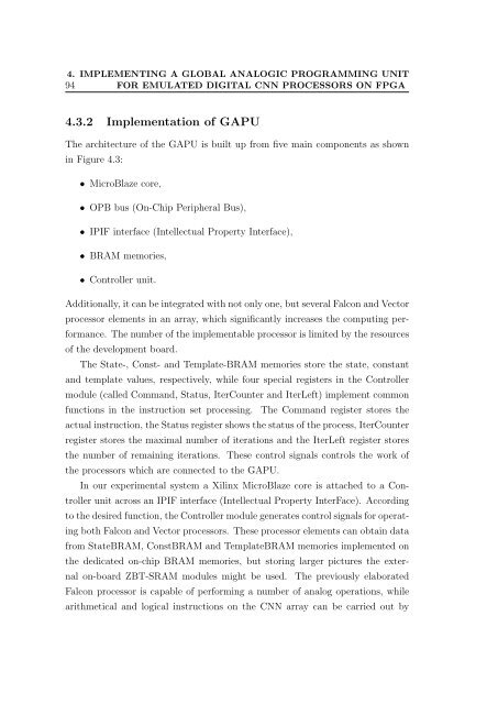
4. IMPLEMENTING A GLOBAL ANALOGIC PROGRAMMING UNIT<br />
94 FOR EMULATED DIGITAL CNN PROCESSORS ON FPGA<br />
4.3.2 Implementation of GAPU<br />
The architecture of the GAPU is built up from five main components as shown<br />
in Figure 4.3:<br />
• MicroBlaze core,<br />
• OPB bus (On-Chip Peripheral Bus),<br />
• IPIF interface (Intellectual Property Interface),<br />
• BRAM memories,<br />
• Controller unit.<br />
Additionally, it can be integrated with not only one, but several Falcon <strong>and</strong> Vector<br />
processor elements in an array, which significantly increases the computing performance.<br />
The number of the implementable processor is limited by the resources<br />
of the development board.<br />
The State-, Const- <strong>and</strong> Template-BRAM memories store the state, constant<br />
<strong>and</strong> template values, respectively, while four special registers in the Controller<br />
module (called Comm<strong>and</strong>, Status, IterCounter <strong>and</strong> IterLeft) implement common<br />
functions in the instruction set processing. The Comm<strong>and</strong> register stores the<br />
actual instruction, the Status register shows the status of the process, IterCounter<br />
register stores the maximal number of iterations <strong>and</strong> the IterLeft register stores<br />
the number of remaining iterations. These control signals controls the work of<br />
the processors which are connected to the GAPU.<br />
In our experimental system a Xilinx MicroBlaze core is attached to a Controller<br />
unit across an IPIF interface (Intellectual Property InterFace). According<br />
to the desired function, the Controller module generates control signals for operating<br />
both Falcon <strong>and</strong> Vector processors. These processor elements can obtain data<br />
from StateBRAM, ConstBRAM <strong>and</strong> TemplateBRAM memories implemented on<br />
the dedicated on-chip BRAM memories, but storing larger pictures the external<br />
on-board ZBT-SRAM modules might be used. The previously elaborated<br />
Falcon processor is capable of performing a number of analog operations, while<br />
arithmetical <strong>and</strong> logical instructions on the CNN array can be carried out by

![optika tervezés [Kompatibilitási mód] - Ez itt...](https://img.yumpu.com/45881475/1/190x146/optika-tervezacs-kompatibilitasi-mad-ez-itt.jpg?quality=85)