PPKE ITK PhD and MPhil Thesis Classes
PPKE ITK PhD and MPhil Thesis Classes
PPKE ITK PhD and MPhil Thesis Classes

You also want an ePaper? Increase the reach of your titles
YUMPU automatically turns print PDFs into web optimized ePapers that Google loves.
26 1. INTRODUCTION<br />
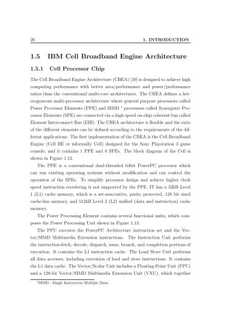
1.5 IBM Cell Broadb<strong>and</strong> Engine Architecture<br />
1.5.1 Cell Processor Chip<br />
The Cell Broadb<strong>and</strong> Engine Architecture (CBEA) [39] is designed to achieve high<br />
computing performance with better area/performance <strong>and</strong> power/performance<br />
ratios than the conventional multi-core architectures. The CBEA defines a heterogeneous<br />
multi-processor architecture where general purpose processors called<br />
Power Processor Elements (PPE) <strong>and</strong> SIMD 1 processors called Synergistic Processor<br />
Elements (SPE) are connected via a high speed on-chip coherent bus called<br />
Element Interconnect Bus (EIB). The CBEA architecture is flexible <strong>and</strong> the ratio<br />
of the different elements can be defined according to the requirements of the different<br />
applications. The first implementation of the CBEA is the Cell Broadb<strong>and</strong><br />
Engine (Cell BE or informally Cell) designed for the Sony Playstation 3 game<br />
console, <strong>and</strong> it contains 1 PPE <strong>and</strong> 8 SPEs. The block diagram of the Cell is<br />
shown in Figure 1.12.<br />
The PPE is a conventional dual-threaded 64bit PowerPC processor which<br />
can run existing operating systems without modification <strong>and</strong> can control the<br />
operation of the SPEs. To simplify processor design <strong>and</strong> achieve higher clock<br />
speed instruction reordering is not supported by the PPE. IT has a 32kB Level<br />
1 (L1) cache memory, which is a set-associative, parity protected, 128 bit sized<br />
cache-line memory, <strong>and</strong> 512kB Level 2 (L2) unified (data <strong>and</strong> instruction) cache<br />
memory.<br />
The Power Processing Element contains several functional units, which composes<br />
the Power Processing Unit shown in Figure 1.13.<br />
The PPU executes the PowerPC Architecture instruction set <strong>and</strong> the Vector/SIMD<br />
Multimedia Extension instructions. The Instruction Unit performs<br />
the instruction-fetch, decode, dispatch, issue, branch, <strong>and</strong> completion portions of<br />
execution. It contains the L1 instruction cache. The Load Store Unit performs<br />
all data accesses, including execution of load <strong>and</strong> store instructions. It contains<br />
the L1 data cache. The Vector/Scalar Unit includes a Floating-Point Unit (FPU)<br />
<strong>and</strong> a 128-bit Vector/SIMD Multimedia Extension Unit (VXU), which together<br />
1 SIMD - Single Instruction Multiple Data

![optika tervezés [Kompatibilitási mód] - Ez itt...](https://img.yumpu.com/45881475/1/190x146/optika-tervezacs-kompatibilitasi-mad-ez-itt.jpg?quality=85)