
Create successful ePaper yourself
Turn your PDF publications into a flip-book with our unique Google optimized e-Paper software.
Philips Semiconductors Preliminary <strong>User</strong> <strong>Manual</strong><br />
ARM-based Microcontroller<br />
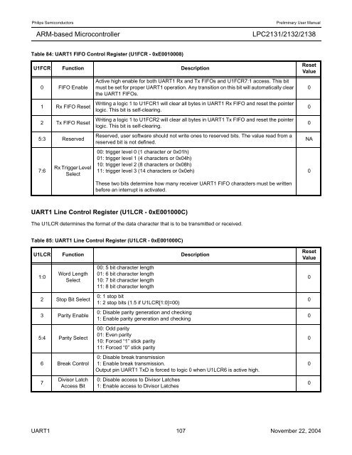
Table 84: UART1 FIFO Control Register (U1FCR - 0xE0010008)<br />
U1FCR Function Description<br />
0 FIFO Enable<br />
1 Rx FIFO Reset<br />
2 Tx FIFO Reset<br />
5:3 Reserved<br />
7:6<br />
Rx Trigger Level<br />
Select<br />
UART1 Line Control Register (U1LCR - 0xE001000C)<br />
The U1LCR determines the format of the data character that is to be transmitted or received.<br />
<strong>LPC2131</strong>/<strong>2132</strong>/<strong>2138</strong><br />
Active high enable for both UART1 Rx and Tx FIFOs and U1FCR7:1 access. This bit<br />
must be set for proper UART1 operation. Any transition on this bit will automatically clear<br />
the UART1 FIFOs.<br />
Writing a logic 1 to U1FCR1 will clear all bytes in UART1 Rx FIFO and reset the pointer<br />
logic. This bit is self-clearing.<br />
Writing a logic 1 to U1FCR2 will clear all bytes in UART1 Tx FIFO and reset the pointer<br />
logic. This bit is self-clearing.<br />
Reserved, user software should not write ones to reserved bits. The value read from a<br />
reserved bit is not defined.<br />
00: trigger level 0 (1 character or 0x01h)<br />
01: trigger level 1 (4 characters or 0x04h)<br />
10: trigger level 2 (8 characters or 0x08h)<br />
11: trigger level 3 (14 characters or 0x0eh)<br />
These two bits determine how many receiver UART1 FIFO characters must be written<br />
before an interrupt is activated.<br />
Table 85: UART1 Line Control Register (U1LCR - 0xE001000C)<br />
U1LCR Function Description<br />
1:0<br />
Word Length<br />
Select<br />
2 Stop Bit Select<br />
3 Parity Enable<br />
5:4 Parity Select<br />
6 Break Control<br />
7<br />
Divisor Latch<br />
Access Bit<br />
00: 5 bit character length<br />
01: 6 bit character length<br />
10: 7 bit character length<br />
11: 8 bit character length<br />
0: 1 stop bit<br />
1: 2 stop bits (1.5 if U1LCR[1:0]=00)<br />
0: Disable parity generation and checking<br />
1: Enable parity generation and checking<br />
00: Odd parity<br />
01: Even parity<br />
10: Forced “1” stick parity<br />
11: Forced “0” stick parity<br />
0: Disable break transmission<br />
1: Enable break transmission.<br />
Output pin UART1 TxD is forced to logic 0 when U1LCR6 is active high.<br />
0: Disable access to Divisor Latches<br />
1: Enable access to Divisor Latches<br />
Reset<br />
Value<br />
UART1 107 November 22, 2004<br />
0<br />
0<br />
0<br />
NA<br />
0<br />
Reset<br />
Value<br />
0<br />
0<br />
0<br />
0<br />
0<br />
0