
Create successful ePaper yourself
Turn your PDF publications into a flip-book with our unique Google optimized e-Paper software.
Philips Semiconductors Preliminary <strong>User</strong> <strong>Manual</strong><br />
ARM-based Microcontroller<br />
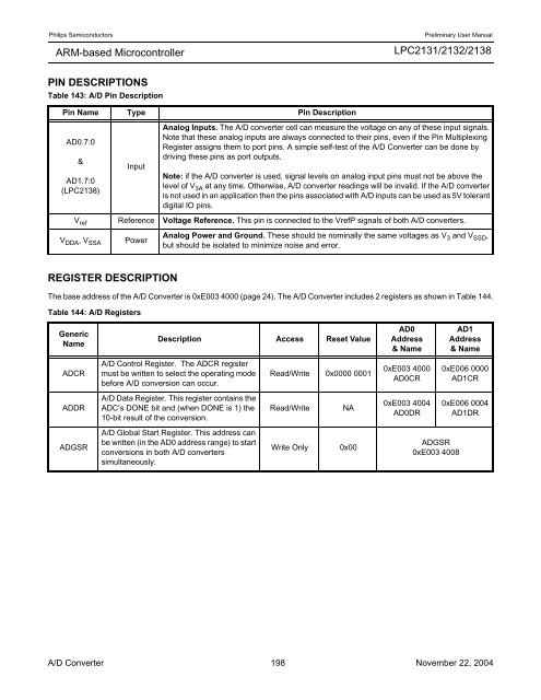
PIN DESCRIPTIONS<br />
Table 143: A/D Pin Description<br />
Pin Name Type Pin Description<br />
AD0.7:0<br />
&<br />
AD1.7:0<br />
(LPC<strong>2138</strong>)<br />
Input<br />
REGISTER DESCRIPTION<br />
<strong>LPC2131</strong>/<strong>2132</strong>/<strong>2138</strong><br />
Analog Inputs. The A/D converter cell can measure the voltage on any of these input signals.<br />
Note that these analog inputs are always connected to their pins, even if the Pin Multiplexing<br />
Register assigns them to port pins. A simple self-test of the A/D Converter can be done by<br />
driving these pins as port outputs.<br />
Note: if the A/D converter is used, signal levels on analog input pins must not be above the<br />
level of V 3A at any time. Otherwise, A/D converter readings will be invalid. If the A/D converter<br />
is not used in an application then the pins associated with A/D inputs can be used as 5V tolerant<br />
digital IO pins.<br />
V ref Reference Voltage Reference. This pin is connected to the VrefP signals of both A/D converters.<br />
V DDA , V SSA<br />
Power<br />
The base address of the A/D Converter is 0xE003 4000 (page 24). The A/D Converter includes 2 registers as shown in Table 144.<br />
Table 144: A/D Registers<br />
Generic<br />
Name<br />
ADCR<br />
ADDR<br />
ADGSR<br />
Analog Power and Ground. These should be nominally the same voltages as V 3 and V SSD ,<br />
but should be isolated to minimize noise and error.<br />
Description Access Reset Value<br />
A/D Control Register. The ADCR register<br />
must be written to select the operating mode<br />
before A/D conversion can occur.<br />
A/D Data Register. This register contains the<br />
ADC’s DONE bit and (when DONE is 1) the<br />
10-bit result of the conversion.<br />
A/D Global Start Register. This address can<br />
be written (in the AD0 address range) to start<br />
conversions in both A/D converters<br />
simultaneously.<br />
Read/Write 0x0000 0001<br />
Read/Write NA<br />
Write Only 0x00<br />
AD0<br />
Address<br />
& Name<br />
0xE003 4000<br />
AD0CR<br />
0xE003 4004<br />
AD0DR<br />
ADGSR<br />
0xE003 4008<br />
AD1<br />
Address<br />
& Name<br />
0xE006 0000<br />
AD1CR<br />
0xE006 0004<br />
AD1DR<br />
A/D Converter 198 November 22, 2004