
Create successful ePaper yourself
Turn your PDF publications into a flip-book with our unique Google optimized e-Paper software.
Philips Semiconductors Preliminary <strong>User</strong> <strong>Manual</strong><br />
ARM-based Microcontroller<br />
REGISTER DESCRIPTION<br />
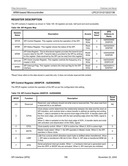
The SPI contains 5 registers as shown in Table 109. All registers are byte, half word and word accessible.<br />
Table 109: SPI Register Map<br />
Generic<br />
Name<br />
*Reset Value refers to the data stored in used bits only. It does not include reserved bits content.<br />
SPI Control Register (S0SPCR - 0xE0020000)<br />
Description Access<br />
SPCR SPI Control Register. This register controls the operation of the SPI.<br />
SPSR SPI Status Register. This register shows the status of the SPI.<br />
SPDR<br />
SPCCR<br />
SPINT<br />
SPI Data Register. This bi-directional register provides the transmit and<br />
receive data for the SPI. Transmit data is provided to the SPI by writing<br />
to this register. Data received by the SPI can be read from this register.<br />
SPI Clock Counter Register. This register controls the frequency of a<br />
master’s SCK.<br />
SPI Interrupt Flag. This register contains the interrupt flag for the SPI<br />
interface.<br />
The SPCR register controls the operation of the SPI as per the configuration bits setting.<br />
Table 110: SPI Control Register (S0SPCR - 0xE0020000)<br />
SPCR Function Description<br />
2:0 Reserved<br />
3 CPHA<br />
<strong>LPC2131</strong>/<strong>2132</strong>/<strong>2138</strong><br />
Reset<br />
Value*<br />
SPI0<br />
Address &<br />
Name<br />
SPI Interface (SPI0) 158 November 22, 2004<br />
Read/<br />
Write<br />
Read<br />
Only<br />
Read/<br />
Write<br />
Read/<br />
Write<br />
Read/<br />
Write<br />
Reserved, user software should not write ones to reserved bits. The value read from<br />
a reserved bit is not defined.<br />
Clock phase control determines the relationship between the data and the clock on<br />
SPI transfers, and controls when a slave transfer is defined as starting and ending.<br />
When 1, data is sampled on the second clock edge of the SCK. A transfer starts with<br />
the first clock edge, and ends with the last sampling edge when the SSEL signal is<br />
active.<br />
When 0, data is sampled on the first clock edge of SCK. A transfer starts and ends<br />
with activation and deactivation of the SSEL signal.<br />
0<br />
0<br />
0<br />
0<br />
0<br />
0xE0020000<br />
S0SPCR<br />
0xE0020004<br />
S0SPSR<br />
0xE0020008<br />
S0SPDR<br />
0xE002000C<br />
S0SPCCR<br />
0xE002001C<br />
S0SPINT<br />
4 CPOL Clock polarity control. When 1, SCK is active low. When 0, SCK is active high. 0<br />
5 MSTR<br />
6 LSBF<br />
7 SPIE<br />
Master mode select. When 1, the SPI operates in Master mode. When 0, the SPI<br />
operates in Slave mode.<br />
LSB First controls which direction each byte is shifted when transferred. When<br />
1, SPI data is transferred LSB (bit 0) first. When 0, SPI data is transferred MSB (bit<br />
7) first.<br />
Serial peripheral interrupt enable. When 1, a hardware interrupt is generated each<br />
time the SPIF or MODF bits are activated. When 0, SPI interrupts are inhibited.<br />
Reset<br />
Value<br />
NA<br />
0<br />
0<br />
0<br />
0