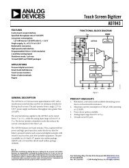

You also want an ePaper? Increase the reach of your titles
YUMPU automatically turns print PDFs into web optimized ePapers that Google loves.
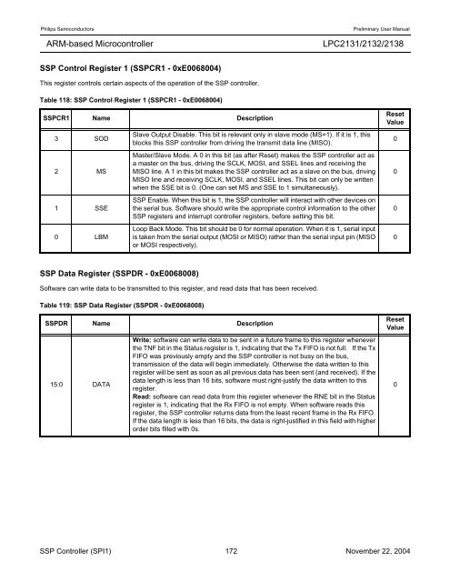
Philips Semiconductors Preliminary <strong>User</strong> <strong>Manual</strong><br />
ARM-based Microcontroller<br />
SSP Control Register 1 (SSPCR1 - 0xE0068004)<br />
This register controls certain aspects of the operation of the SSP controller.<br />
Table 118: SSP Control Register 1 (SSPCR1 - 0xE0068004)<br />
SSPCR1 Name Description<br />
3 SOD<br />
2 MS<br />
1 SSE<br />
0 LBM<br />
SSP Data Register (SSPDR - 0xE0068008)<br />
Software can write data to be transmitted to this register, and read data that has been received.<br />
Table 119: SSP Data Register (SSPDR - 0xE0068008)<br />
<strong>LPC2131</strong>/<strong>2132</strong>/<strong>2138</strong><br />
Slave Output Disable. This bit is relevant only in slave mode (MS=1). If it is 1, this<br />
blocks this SSP controller from driving the transmit data line (MISO).<br />
Master/Slave Mode. A 0 in this bit (as after Reset) makes the SSP controller act as<br />
a master on the bus, driving the SCLK, MOSI, and SSEL lines and receiving the<br />
MISO line. A 1 in this bit makes the SSP controller act as a slave on the bus, driving<br />
MISO line and receiving SCLK, MOSI, and SSEL lines. This bit can only be written<br />
when the SSE bit is 0. (One can set MS and SSE to 1 simultaneously).<br />
SSP Enable. When this bit is 1, the SSP controller will interact with other devices on<br />
the serial bus. Software should write the appropriate control information to the other<br />
SSP registers and interrupt controller registers, before setting this bit.<br />
Loop Back Mode. This bit should be 0 for normal operation. When it is 1, serial input<br />
is taken from the serial output (MOSI or MISO) rather than the serial input pin (MISO<br />
or MOSI respectively).<br />
SSPDR Name Description<br />
15:0 DATA<br />
Write: software can write data to be sent in a future frame to this register whenever<br />
the TNF bit in the Status register is 1, indicating that the Tx FIFO is not full. If the Tx<br />
FIFO was previously empty and the SSP controller is not busy on the bus,<br />
transmission of the data will begin immediately. Otherwise the data written to this<br />
register will be sent as soon as all previous data has been sent (and received). If the<br />
data length is less than 16 bits, software must right-justify the data written to this<br />
register.<br />
Read: software can read data from this register whenever the RNE bit in the Status<br />
register is 1, indicating that the Rx FIFO is not empty. When software reads this<br />
register, the SSP controller returns data from the least recent frame in the Rx FIFO.<br />
If the data length is less than 16 bits, the data is right-justified in this field with higher<br />
order bits filled with 0s.<br />
Reset<br />
Value<br />
SSP Controller (SPI1) 172 November 22, 2004<br />
0<br />
0<br />
0<br />
0<br />
Reset<br />
Value<br />
0