
Create successful ePaper yourself
Turn your PDF publications into a flip-book with our unique Google optimized e-Paper software.
Philips Semiconductors Preliminary <strong>User</strong> <strong>Manual</strong><br />
ARM-based Microcontroller<br />
the CLK signal is forced LOW<br />
SSEL is forced HIGH<br />
the transmit MOSI/MISO pad is in high impedance<br />
<strong>LPC2131</strong>/<strong>2132</strong>/<strong>2138</strong><br />
If the SSP is enabled and there is valid data within the transmit FIFO, the start of transmission is signified by the SSEL master<br />
signal being driven LOW. This causes slave data to be enabled onto the MISO input line of the master. Master’s MOSI is enabled.<br />
One half SCK period later, valid master data is transferred to the MOSI pin. Now that both the master and slave data have been<br />
set, the SCK master clock pin goes HIGH after one further half SCK period.<br />
The data is now captured on the rising and propagated on the falling edges of the SCK signal.<br />
In the case of a single word transmission, after all bits of the data word have been transferred, the SSEL line is returned to its<br />
idle HIGH state one SCK period after the last bit has been captured.<br />
However, in the case of continuous back-to-back transmissions, the SSEL signal must be pulsed HIGH between each data word<br />
transfer. This is because the slave select pin freezes the data in its serial peripheral register and does not allow it to be altered<br />
if the CPHA bit is logic zero. Therefore the master device must raise the SSEL pin of the slave device between each data transfer<br />
to enable the serial peripheral data write. On completion of the continuous transfer, the SSEL pin is returned to its idle state one<br />
SCK period after the last bit has been captured.<br />
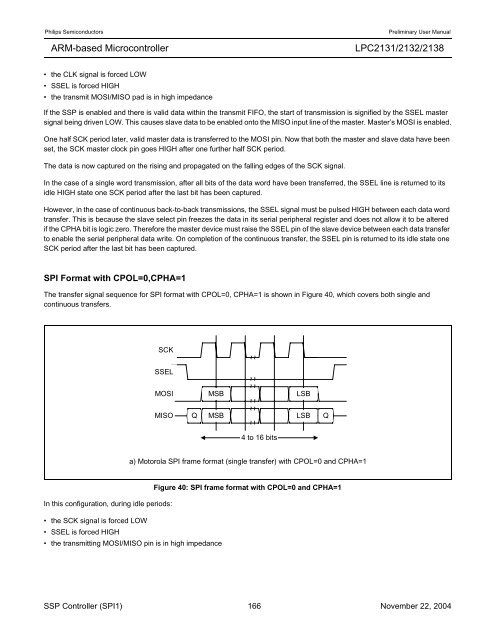
SPI Format with CPOL=0,CPHA=1<br />
The transfer signal sequence for SPI format with CPOL=0, CPHA=1 is shown in Figure 40, which covers both single and<br />
continuous transfers.<br />
SCK<br />
SSEL<br />
In this configuration, during idle periods:<br />
MOSI MSB<br />
MISO Q<br />
MSB<br />
the SCK signal is forced LOW<br />
SSEL is forced HIGH<br />
the transmitting MOSI/MISO pin is in high impedance<br />
~<br />
~ ~ ~<br />
~<br />
~<br />
4 to 16 bits<br />
a) Motorola SPI frame format (single transfer) with CPOL=0 and CPHA=1<br />
Figure 40: SPI frame format with CPOL=0 and CPHA=1<br />
SSP Controller (SPI1) 166 November 22, 2004<br />
LSB<br />
LSB Q