
Create successful ePaper yourself
Turn your PDF publications into a flip-book with our unique Google optimized e-Paper software.
Philips Semiconductors Preliminary <strong>User</strong> <strong>Manual</strong><br />
ARM-based Microcontroller<br />
REGISTER DESCRIPTIONS<br />
<strong>LPC2131</strong>/<strong>2132</strong>/<strong>2138</strong><br />
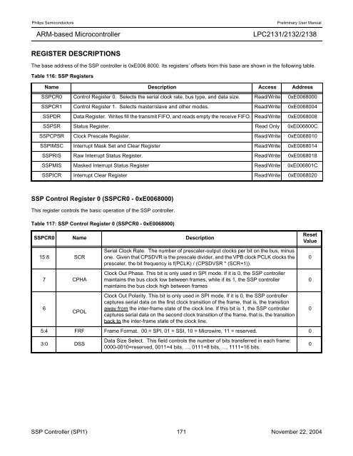
The base address of the SSP controller is 0xE006 8000. Its registers’ offsets from this base are shown in the following table.<br />
Table 116: SSP Registers<br />
Name Description Access Address<br />
SSPCR0 Control Register 0. Selects the serial clock rate, bus type, and data size. Read/Write 0xE0068000<br />
SSPCR1 Control Register 1. Selects master/slave and other modes. Read/Write 0xE0068004<br />
SSPDR Data Register. Writes fill the transmit FIFO, and reads empty the receive FIFO. Read/Write 0xE0068008<br />
SSPSR Status Register. Read Only 0xE006800C<br />
SSPCPSR Clock Prescale Register. Read/Write 0xE0068010<br />
SSPIMSC Interrupt Mask Set and Clear Register Read/Write 0xE0068014<br />
SSPRIS Raw Interrupt Status Register. Read/Write 0xE0068018<br />
SSPMIS Masked Interrupt Status Register Read/Write 0xE006801C<br />
SSPICR Interrupt Clear Register Read/Write 0xE0068020<br />
SSP Control Register 0 (SSPCR0 - 0xE0068000)<br />
This register controls the basic operation of the SSP controller.<br />
Table 117: SSP Control Register 0 (SSPCR0 - 0xE0068000)<br />
SSPCR0 Name Description<br />
15:8 SCR<br />
7 CPHA<br />
6<br />
CPOL<br />
Serial Clock Rate. The number of prescaler-output clocks per bit on the bus, minus<br />
one. Given that CPSDVR is the prescale divider, and the VPB clock PCLK clocks the<br />
prescaler, the bit frequency is f(PCLK) / (CPSDVSR * (SCR+1)).<br />
Clock Out Phase. This bit is only used in SPI mode. If it is 0, the SSP controller<br />
maintains the bus clock low between frames, while if its 1, the SSP controller<br />
maintains the bus clock high between frames<br />
Clock Out Polarity. This bit is only used in SPI mode. If it is 0, the SSP controller<br />
captures serial data on the first clock transition of the frame, that is, the transition<br />
away from the inter-frame state of the clock line. If this bit is 1, the SSP controller<br />
captures serial data on the second clock transition of the frame, that is, the transition<br />
back to the inter-frame state of the clock line.<br />
5:4 FRF Frame Format. 00 = SPI, 01 = SSI, 10 = Microwire, 11 = reserved. 0<br />
3:0 DSS<br />
Data Size Select. This field controls the number of bits transferred in each frame:<br />
0000-0010=reserved, 0011=4 bits, ..., 0111=8 bits, ..., 1111=16 bits.<br />
Reset<br />
Value<br />
SSP Controller (SPI1) 171 November 22, 2004<br />
0<br />
0<br />
0<br />
0