
You also want an ePaper? Increase the reach of your titles
YUMPU automatically turns print PDFs into web optimized ePapers that Google loves.
Philips Semiconductors Preliminary <strong>User</strong> <strong>Manual</strong><br />
ARM-based Microcontroller<br />
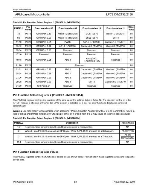
Table 51: Pin Function Select Register 1 (PINSEL1 - 0xE002C004)<br />
PINSEL1<br />
Pin<br />
Name<br />
Pin Function Select Register 2 (PINSEL2 - 0xE002C014)<br />
<strong>LPC2131</strong>/<strong>2132</strong>/<strong>2138</strong><br />
Function when 00 Function when 01 Function when 10 Function when 11<br />
7:6 P0.19 GPIO Port 0.19 Match 1.2 (TIMER1) MOSI (SSP) Match 1.3 (TIMER1) 00<br />
9:8 P0.20 GPIO Port 0.20 Match 1.3 (TIMER1) SSEL (SSP) EINT3 00<br />
11:10 P0.21 GPIO Port 0.21 PWM5 AD1.6 (LPC<strong>2138</strong>) Capture 1.3 (TIMER1) 00<br />
13:12 P0.22 GPIO Port 0.22 AD1.7 (LPC<strong>2138</strong>) Capture 0.0 (TIMER0) Match 0.0 (TIMER0) 00<br />
15:14 P0.23 GPIO Port 0.23 Reserved Reserved Reserved 00<br />
17:16 P0.24 Reserved Reserved Reserved Reserved 00<br />
19:18 P0.25 GPIO Port 0.25 AD0.4<br />
Aout (DAC)<br />
(LPC<strong>2132</strong>/<strong>2138</strong>)<br />
Reserved 00<br />
21:20 P0.26 Reserved 00<br />
23:22 P0.27 GPIO Port 0.27 AD0.0 Capture 0.1 (TIMER0) Match 0.1 (TIMER0) 00<br />
25:24 P0.28 GPIO Port 0.28 AD0.1 Capture 0.2 (TIMER0) Match 0.2 (TIMER0) 00<br />
27:26 P0.29 GPIO Port 0.29 AD0.2 Capture 0.3 (TIMER0) Match 0.3 (TIMER0) 00<br />
29:28 P0.30 GPIO Port 0.30 AD0.3 EINT3 Capture 0.0 (TIMER0) 00<br />
31:30 P0.31 GPI Port 0.31 Reserved Reserved Reserved 00<br />
The PINSEL2 register controls the functions of the pins as per the settings listed in Table 52. The direction control bit in the<br />
IO1DIR register is effective only when the GPIO function is selected for a pin. For other functions direction is controlled<br />
automatically.<br />
Warning: use read-modify-write operation when accessing PINSEL2 register. Accidental write of 0 to bit 2 and/or bit 3 results in<br />
loss of debug and/or trace functionality! Changing of either bit 4 or bit 5 from 1 to 0 may cause an incorrect code execution!<br />
Table 52: Pin Function Select Register 2 (PINSEL2 - 0xE002C014)<br />
PINSEL2 Description Reset Value<br />
1:0 Reserved. <strong>User</strong> software should should not write ones to reserved bits. NA<br />
2 When 0, pins P1.36:26 are used as GPIO pins. When 1, P1.31:26 are used as a Debug port. P1.26/RTCK<br />
3 When 0, pins P1.25:16 are used as GPIO pins. When 1, P1.25:16 are used as a Trace port.<br />
Pin Function Select Register Values<br />
P1.20/<br />
TRACESYNC<br />
31:4 Reserved. <strong>User</strong> software should should not write ones to reserved bits. NA<br />
Reset<br />
Value<br />
The PINSEL registers control the functions of device pins as shown below. Pairs of bits in these registers correspond to specific<br />
device pins.<br />
Pin Connect Block 83 November 22, 2004