
You also want an ePaper? Increase the reach of your titles
YUMPU automatically turns print PDFs into web optimized ePapers that Google loves.
Philips Semiconductors Preliminary <strong>User</strong> <strong>Manual</strong><br />
ARM-based Microcontroller<br />
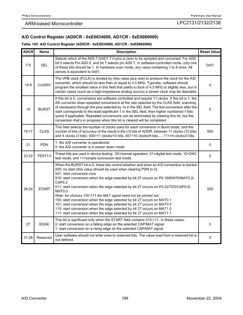
A/D Control Register (AD0CR - 0xE0034000, AD1CR - 0xE0060000)<br />
Table 145: A/D Control Register (AD0CR - 0xE0034000, AD1CR - 0xE0060000)<br />
<strong>LPC2131</strong>/<strong>2132</strong>/<strong>2138</strong><br />
ADCR Name Description Reset Value<br />
7:0 SEL<br />
15:8 CLKDIV<br />
16 BURST<br />
19:17 CLKS<br />
21 PDN<br />
23:22 TEST1:0<br />
26:24 START<br />
27 EDGE<br />
31:28 Reserved<br />
Selects which of the AD0.7:0/AD1.7:0 pins is (are) to be sampled and converted. For AD0,<br />
bit 0 selects Pin AD0.0, and bit 7 selects pin AD0.7. In software-controlled mode, only one<br />
of these bits should be 1. In hardware scan mode, any value containing 1 to 8 ones. All<br />
zeroes is equivalent to 0x01.<br />
The VPB clock (PCLK) is divided by (this value plus one) to produce the clock for the A/D<br />
converter, which should be less than or equal to 4.5 MHz. Typically, software should<br />
program the smallest value in this field that yields a clock of 4.5 MHz or slightly less, but in<br />
certain cases (such as a high-impedance analog source) a slower clock may be desirable.<br />
If this bit is 0, conversions are software controlled and require 11 clocks. If this bit is 1, the<br />
AD converter does repeated conversions at the rate selected by the CLKS field, scanning<br />
(if necessary) through the pins selected by 1s in the SEL field. The first conversion after the<br />
start corresponds to the least-significant 1 in the SEL field, then higher numbered 1-bits<br />
(pins) if applicable. Repeated conversions can be terminated by clearing this bit, but the<br />
conversion that’s in progress when this bit is cleared will be completed.<br />
This field selects the number of clocks used for each conversion in Burst mode, and the<br />
number of bits of accuracy of the result in the LS bits of ADDR, between 11 clocks (10 bits)<br />
and 4 clocks (3 bits): 000=11 clocks/10 bits, 001=10 clocks/9 bits,..., 111=4 clocks/3 bits<br />
1: the A/D converter is operational<br />
0: the A/D converter is in power down mode<br />
These bits are used in device testing. 00=normal operation, 01=digital test mode, 10=DAC<br />
test mode, and 11=simple conversion test mode.<br />
When the BURST bit is 0, these bits control whether and when an A/D conversion is started:<br />
000: no start (this value should be used when clearing PDN to 0)<br />
001: start conversion now<br />
010: start conversion when the edge selected by bit 27 occurs on P0.16/EINT0/MAT0.2/<br />
CAP0.2<br />
011: start conversion when the edge selected by bit 27 occurs on P0.22/TD3/CAP0.0/<br />
MAT0.0<br />
Note: for choices 100-111 the MAT signal need not be pinned out:<br />
100: start conversion when the edge selected by bit 27 occurs on MAT0.1<br />
101: start conversion when the edge selected by bit 27 occurs on MAT0.3<br />
110: start conversion when the edge selected by bit 27 occurs on MAT1.0<br />
111: start conversion when the edge selected by bit 27 occurs on MAT1.1<br />
This bit is significant only when the START field contains 010-111. In these cases:<br />
0: start conversion on a falling edge on the selected CAP/MAT signal<br />
1: start conversion on a rising edge on the selected CAP/MAT signal<br />
<strong>User</strong> software should not write ones to reserved bits. The value read from a reserved bit is<br />
not defined.<br />
A/D Converter 199 November 22, 2004<br />
0x01<br />
0<br />
0<br />
000<br />
0<br />
0<br />
000<br />
0<br />
0