
You also want an ePaper? Increase the reach of your titles
YUMPU automatically turns print PDFs into web optimized ePapers that Google loves.
Philips Semiconductors Preliminary <strong>User</strong> <strong>Manual</strong><br />
ARM-based Microcontroller<br />
DESCRIPTION<br />
<strong>LPC2131</strong>/<strong>2132</strong>/<strong>2138</strong><br />
The Timer/Counter is designed to count cycles of the peripheral clock (pclk) or an externally-supplied clock, and can optionally<br />
generate interrupts or perform other actions at specified timer values, based on four match registers. It also includes four capture<br />
inputs to trap the timer value when an input signal transitions, optionally generating an interrupt.<br />
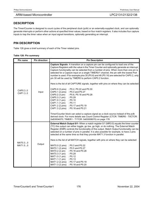
PIN DESCRIPTION<br />
Table 126 gives a brief summary of each of the Timer related pins.<br />
Table 126: Pin summary<br />
Pin name Pin direction Pin Description<br />
CAP0.3..0<br />
CAP1.3..0<br />
MAT0.3...0<br />
MAT1.0...0<br />
Input<br />
Output<br />
Capture Signals- A transition on a capture pin can be configured to load one of the<br />
Capture Registers with the value in the Timer Counter and optionally generate an interrupt.<br />
Capture functionality can be selected from a number of pins. When more than one pin is<br />
selected for a Capture input on a single TIMER0/1 channel, the pin with the lowest Port<br />
number is used. If for example pins 30 (P0.6) and 46 (P0.16) are selected for CAP0.2, only<br />
pin 30 will be used by TIMER0 to perform CAP0.2 function.<br />
Here is the list of all CAPTURE signals, together with pins on where they can be selected:<br />
CAP0.0 (3 pins) : P0.2, P0.22 and P0.30<br />
CAP0.1 (2 pins) : P0.4 and P0.27<br />
CAP0.2 (3 pin) : P0.6, P0.16 and P0.28<br />
CAP0.3 (1 pin): : P0.29<br />
CAP1.0 (1 pin): : P0.10<br />
CAP1.1 (1 pin): : P0.11<br />
CAP1.2 (2 pins) : P0.17 and P0.19<br />
CAP1.3 (2 pins) : P0.18 and P0.21<br />
Timer/Counter block can select a capture signal as a clock source instead of the pclk<br />
derived clock. For more details see Count Control Register (CTCR: TIMER0 - T0CTCR:<br />
0xE0004070; TIMER1 - T1TCR: 0xE0008070) on page 178<br />
External Match Output 0/1- When a match register 0/1 (MR3:0) equals the timer counter<br />
(TC) this output can either toggle, go low, go high, or do nothing. The External Match<br />
Register (EMR) controls the functionality of this output. Match Output functionality can be<br />
selected on a number of pins in parallel. It is also possible for example, to have 2 pins<br />
selected at the same time so that they provide MAT1.3 function in parallel.<br />
Here is the list of all MATCH signals, together with pins on where they can be selected:<br />
MAT0.0 (2 pins) : P0.3 and P0.22<br />
MAT0.1 (2 pins) : P0.5 and P0.27<br />
MAT0.2 (2 pin) : P0.16 and P0.28<br />
MAT0.3 (1 pin): : P0.29<br />
MAT1.0 (1 pin): : P0.12<br />
MAT1.1 (1 pin): : P0.13<br />
MAT1.2 (2 pins) : P0.17 and P0.19<br />
MAT1.3 (2 pins) : P0.18 and P0.20<br />
Timer/Counter0 and Timer/Counter1 176 November 22, 2004