
You also want an ePaper? Increase the reach of your titles
YUMPU automatically turns print PDFs into web optimized ePapers that Google loves.
Philips Semiconductors Preliminary <strong>User</strong> <strong>Manual</strong><br />
ARM-based Microcontroller<br />
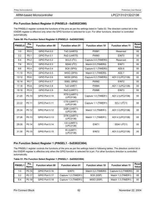
Pin Function Select Register 0 (PINSEL0 - 0xE002C000)<br />
<strong>LPC2131</strong>/<strong>2132</strong>/<strong>2138</strong><br />
The PINSEL0 register controls the functions of the pins as per the settings listed in Table 53. The direction control bit in the<br />
IO0DIR register is effective only when the GPIO function is selected for a pin. For other functions, direction is controlled<br />
automatically.<br />
Table 50: Pin Function Select Register 0 (PINSEL0 - 0xE002C000)<br />
PINSEL0<br />
Pin<br />
Name<br />
Function when 00 Function when 01 Function when 10 Function when 11<br />
1:0 P0.0 GPIO Port 0.0 TxD (UART0) PWM1 Reserved 00<br />
3:2 P0.1 GPIO Port 0.1 RxD (UART0) PWM3 EINT0 00<br />
5:4 P0.2 GPIO Port 0.2 SCL0 (I 2 C) Capture 0.0 (TIMER0) Reserved 00<br />
7:6 P0.3 GPIO Port 0.3 SDA0 (I 2 C) Match 0.0 (TIMER0) EINT1 00<br />
9:8 P0.4 GPIO Port 0.4 SCK (SPI0) Capture 0.1 (TIMER0) AD0.6 00<br />
11:10 P0.5 GPIO Port 0.5 MISO (SPI0) Match 0.1 (TIMER0) AD0.7 00<br />
13:12 P0.6 GPIO Port 0.6 MOSI (SPI0) Capture 0.2 (TIMER0) AD1.0 (LPC<strong>2138</strong>) 00<br />
15:14 P0.7 GPIO Port 0.7 SSEL (SPI0) PWM2 EINT2 00<br />
17:16 P0.8 GPIO Port 0.8 TxD UART1 PWM4 AD1.1 (LPC<strong>2138</strong>) 00<br />
19:18 P0.9 GPIO Port 0.9 RxD (UART1) PWM6 EINT3 00<br />
21:20 P0.10 GPIO Port 0.10<br />
23:22 P0.11 GPIO Port 0.11<br />
25:24 P0.12 GPIO Port 0.12<br />
27:26 P0.13 GPIO Port 0.13<br />
29:28 P0.14 GPIO Port 0.14<br />
31:30 P0.15 GPIO Port 0.15<br />
RTS (UART1)<br />
(LPC<strong>2138</strong>)<br />
CTS (UART1)<br />
(LPC<strong>2138</strong>)<br />
DSR (UART1)<br />
(LPC<strong>2138</strong>)<br />
DTR (UART1)<br />
(LPC<strong>2138</strong>)<br />
CD (UART1)<br />
(LPC<strong>2138</strong>)<br />
RI (UART1<br />
(LPC<strong>2138</strong>)<br />
Pin Function Select Register 1 (PINSEL1 - 0xE002C004)<br />
The PINSEL1 register controls the functions of the pins as per the settings listed in following tables. The direction control bit in<br />
the IO0DIR register is effective only when the GPIO function is selected for a pin. For other functions direction is controlled<br />
automatically.<br />
Table 51: Pin Function Select Register 1 (PINSEL1 - 0xE002C004)<br />
PINSEL1<br />
Pin<br />
Name<br />
Reset<br />
Value<br />
Capture 1.0 (TIMER1) AD1.2 (LPC<strong>2138</strong>) 00<br />
Capture 1.1 (TIMER1) SCL1 (I 2 C1) 00<br />
Match 1.0 (TIMER1) AD1.3 (LPC<strong>2138</strong>) 00<br />
Match 1.1 (TIMER1) AD1.4 (LPC<strong>2138</strong>) 00<br />
EINT1 SDA1 (I 2 C1) 00<br />
EINT2 AD1.5 (LPC<strong>2138</strong>) 00<br />
Function when 00 Function when 01 Function when 10 Function when 11<br />
1:0 P0.16 GPIO Port 0.16 EINT0 Match 0.2 (TIMER0) Capture 0.2 (TIMER0) 00<br />
3:2 P0.17 GPIO Port 0.17 Capture 1.2 (TIMER1) SCK (SSP) Match 1.2 (TIMER1) 00<br />
5:4 P0.18 GPIO Port 0.18 Capture 1.3 (TIMER1) MISO (SSP) Match 1.3 (TIMER1) 00<br />
Reset<br />
Value<br />
Pin Connect Block 82 November 22, 2004