

Photonic crystals in biology - NanoTR-VI
Photonic crystals in biology - NanoTR-VI
Photonic crystals in biology - NanoTR-VI
- No tags were found...

You also want an ePaper? Increase the reach of your titles
YUMPU automatically turns print PDFs into web optimized ePapers that Google loves.
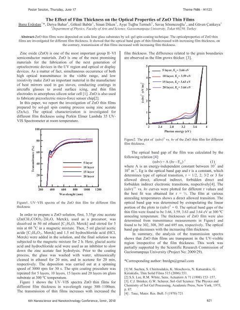
PP mPP vs.P =P,PP (1)P andPoster Session, Thursday, June 17Theme F686 - N1123The Effect of Film Thickness on the Optical Properties of ZnO Th<strong>in</strong> Films111111UBanu ErdoanUP P*, Derya BaharP P, Göknil BabürP P, S<strong>in</strong>an DikenP P, Aye Tuba TermeliP P, Sava SönmezoluPPand Güven ÇankayaP1PDepartment of Physics, Faculty of Arts and Science, Gaziosmanpaa University, Tokat 60250, TurkeyAbstract-ZnO th<strong>in</strong> films were deposited on soda lime glass substrates by sol–gel sp<strong>in</strong>-coat<strong>in</strong>g technique. The opticalproperties of ZnO th<strong>in</strong>films are <strong>in</strong>vestigated for different film thickness. It showed that the optical band gaps of th<strong>in</strong> filmdecreased with <strong>in</strong>creas<strong>in</strong>g film thickness, onthe contrary, transmission of th<strong>in</strong> films <strong>in</strong>creased with <strong>in</strong>creas<strong>in</strong>g film thickness.1Z<strong>in</strong>c oxide (ZnO) is one of the most important group II–<strong>VI</strong>semiconductor materials. ZnO is one of the most promis<strong>in</strong>gmaterials for the fabrication of the next generation ofoptoelectronic devices <strong>in</strong> the UV region and optical or displaydevices. As a matter of fact, simultaneous occurrence of bothhigh optical transmittance <strong>in</strong> the visble range, and lowresistivity make ZnO an important material <strong>in</strong> the manufactureof heat mirrors used <strong>in</strong> gas stoves, conduct<strong>in</strong>g coat<strong>in</strong>gs <strong>in</strong>aircrafts glasses to avoid surface ic<strong>in</strong>g, and th<strong>in</strong> filmelectrodes <strong>in</strong> amorphous silicon solar cell [1]. ZnO is also usedto fabricate piezoelectric micro-force sensor chip[2].In this paper, we report the <strong>in</strong>vestigation of ZnO th<strong>in</strong> filmsprepared by sol-gel sp<strong>in</strong> coat<strong>in</strong>g process us<strong>in</strong>g z<strong>in</strong>c acetate(ZnAc). The optical characterization is <strong>in</strong>vestigated fordifferent film thickness us<strong>in</strong>g Perk<strong>in</strong> Elmer Lambda 35 UV-<strong>VI</strong>S Spectrometer at room temperature.Transmittance (%)100806040205 layer10 layer15 layer20 layer0200 400 600 800 1000 1200Wavelenght (nm)Figure1. UV–<strong>VI</strong>S spectra of the ZnO th<strong>in</strong> film for different filmthicknessIn order to prepare a ZnO solution, first, 3.35gr z<strong>in</strong>c acetate(Zn(CHR3RCOO)R2R·2HR2RO, Merck), used as a precursor, wasdissolved <strong>in</strong> 50 ml ethanol [CR2RHR6RO, Merck] and stirred for 50m<strong>in</strong> at 60 P PC <strong>in</strong> a magnetic mixture. Then, 5 ml glacial aceticacide [CR2RHR4ROR2R, Merck] and 1.5 ml hydrochloride acid (HCl,Merck) were added <strong>in</strong> the solution, and the f<strong>in</strong>al solution wassubjected to the magnetic mixture for 2 h. Here, glacial aceticacid and hydrochloride acid were used as an <strong>in</strong>hibitor to slowdown the z<strong>in</strong>c acetate fast hydrolysis. Prior to the coat<strong>in</strong>gprocess, the glass was washed with water, ultrasonicallycleaned <strong>in</strong> ethanol for 20 m<strong>in</strong>, and <strong>in</strong> acetone for 20 m<strong>in</strong>,respectively. The deposition was carried out at a sp<strong>in</strong>n<strong>in</strong>gspeed of 3000 rpm for 30 s. The sp<strong>in</strong> coat<strong>in</strong>g procedure wasrepeated for 5 layers, 10 layers, 15 layers and 20 layers on glasssubstrate at 300 ºC temperature.Figure 1 shows the UV–<strong>VI</strong>S spectra ZnO th<strong>in</strong> films fordifferent film thickness <strong>in</strong> wavelength range 300–1100nm.The transmission of th<strong>in</strong> films <strong>in</strong>creases with <strong>in</strong>creased thefilm thickness. The diffrerence related to the gra<strong>in</strong> boundariesare observed as the film grows thicker. [3].(hv) 2 (eV/m) 2543215 layer, E g= 3.66 eV10 layer, E g= 3.59 eV15 layer, E g= 3.63 eV20 layer, E g = 3.64 eV02 2.4 2.8 3.2 3.6 4Photon energy (eV)2Figure2. The plot of (hv)P P vs. hv of the ZnO th<strong>in</strong> film for differentfilm thickness.The optical band gap of the film was calculated by thefollow<strong>in</strong>g relation [4]:r(hv) = A (hv - ERgR) P7where A is an energy-<strong>in</strong>dependent constant between 10P8 -110PP, Eg is the optical band gap and r is a constant, whichdeterm<strong>in</strong>es type of optical transition, r = 1/2, 2, 3/2 or 3 forallowed direct, allowed <strong>in</strong>direct, forbidden direct andforbidden <strong>in</strong>direct electronic transitions, respectively[4]. The1/r(hv)P hv curves were plotted for different r values andthe best fit was obta<strong>in</strong>ed for r = ½. The film at variousanneal<strong>in</strong>g temperatures shows a direct allowed transition. Theoptical band gap was determ<strong>in</strong>ed by extrapolat<strong>in</strong>g the l<strong>in</strong>ear2portion of the plots to (hv)P 0. The optical band gaps of theth<strong>in</strong> film were found to be 3.66, 3.59, 3.63 and 3.64 eV at 300 ºCanneal<strong>in</strong>g temperature. The thicknesses of ZnO film were alsodeterm<strong>in</strong>ed from transmittance measurements <strong>in</strong> Figure1 andfound to be 302, 308, 385 and 695 nm, respectively. The opticalband gap decreases with the <strong>in</strong>creas<strong>in</strong>g film thickness.In summary, the analysis of the transmission spectrashows that ZnO th<strong>in</strong> films are transparent <strong>in</strong> the UV-visibleregion irrespective of the film thickness. This work waspartially supported by the Scientific Research Commission ofGaziosmanpaa University (Project No: 2009/29).*Correspond<strong>in</strong>g author: bnrdgn@gmail.com[1] M. Suchea, S. Chiritoulakis, K. Moschovis, N. Katsarakis, G.Kiriakidis, Th<strong>in</strong> Solid Films 515 (2006) 551.[2] S.S. Lee, R.M. White, Sens. Actuators A 71 (1998) 153–157.[3]. C.J. Br<strong>in</strong>ker, G.W. Scherer, Sol–Gel Science: The Physics andChemistry of Sol Gel Process<strong>in</strong>g, Academic Press, New York, 1975,p. 87.[4] . Tauc, Mater. Res. Bull. 5 (1970) 7216th Nanoscience and Nanotechnology Conference, zmir, 2010 621


