

Photonic crystals in biology - NanoTR-VI
Photonic crystals in biology - NanoTR-VI
Photonic crystals in biology - NanoTR-VI
- No tags were found...

Create successful ePaper yourself
Turn your PDF publications into a flip-book with our unique Google optimized e-Paper software.
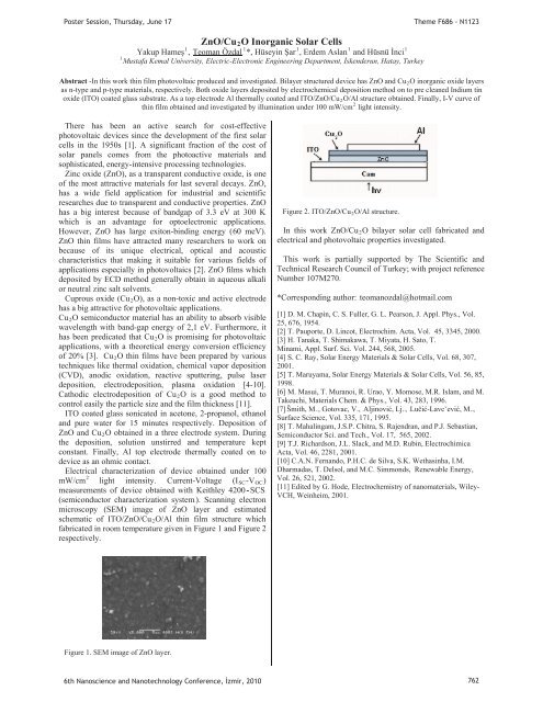
PP lightPoster Session, Thursday, June 17Theme F686 - N1123ZnO/CuR2RO Inorganic Solar Cells1110BYakup HameP P, UTeoman ÖzdalUP P*, Hüsey<strong>in</strong> arP P, Erdem AslanP1P and Hüsnü nci 1PPMustafa Kemal University, Electric-Electronic Eng<strong>in</strong>eer<strong>in</strong>g Department, skenderun, Hatay, Turkey1Abstract -In this work th<strong>in</strong> film photovoltaic produced and <strong>in</strong>vestigated. Bilayer structured device has ZnO and CuR2RO <strong>in</strong>organic oxide layersas n-type and p-type materials, respectively. Both oxide layers deposited by electrochemical deposition method on to pre cleaned Indium t<strong>in</strong>oxide (ITO) coated glass substrate. As a top electrode Al thermally coated and ITO/ZnO/CuR2RO/Al structure obta<strong>in</strong>ed. F<strong>in</strong>ally, I-V curve of2th<strong>in</strong> film obta<strong>in</strong>ed and <strong>in</strong>vestigated by illum<strong>in</strong>ation under 100 mW/cmP <strong>in</strong>tensity.There has been an active search for cost-effectivephotovoltaic devices s<strong>in</strong>ce the development of the first solarcells <strong>in</strong> the 1950s [1]. A significant fraction of the cost ofsolar panels comes from the photoactive materials andsophisticated, energy-<strong>in</strong>tensive process<strong>in</strong>g technologies.Z<strong>in</strong>c oxide (ZnO), as a transparent conductive oxide, is oneof the most attractive materials for last several decays. ZnO,has a wide field application for <strong>in</strong>dustrial and scientificresearches due to transparent and conductive properties. ZnOhas a big <strong>in</strong>terest because of bandgap of 3.3 eV at T300 KTwhich is an advantage for Toptoelectronic applications.However, ZnO has large exiton-b<strong>in</strong>d<strong>in</strong>g energy (T60 meV).ZnO th<strong>in</strong> films have attracted many researchers to work onbecause of its unique electrical, optical and acousticcharacteristics that mak<strong>in</strong>g it suitable for various fields ofapplications especially <strong>in</strong> photovoltaics [2]. ZnO films whichdeposited by ECD method generally obta<strong>in</strong> <strong>in</strong> aqueous alkalior neutral z<strong>in</strong>c salt solvents.Cuprous oxide (CuR2RO), as a non-toxic and active electrodehas a big attractive for photovoltaic applications.CuR2RO semiconductor material has an ability to absorb visiblewavelength with band-gap energy of 2,1 eV. Furthermore, ithas been predicated that CuR2RO is promis<strong>in</strong>g for photovoltaicapplications, with a theoretical energy conversion efficiencyof 20% [3]. CuR2RO th<strong>in</strong> films have been prepared by varioustechniques like thermal oxidation, chemical vapor deposition(CVD), anodic oxidation, reactive sputter<strong>in</strong>g, pulse laserdeposition, electrodeposition, plasma oxidation [4-10].Cathodic electrodeposition of CuR2RO is a good method tocontrol easily the particle size and the film thickness [11].ITO coated glass sonicated <strong>in</strong> acetone, 2-propanol, ethanoland pure water for 15 m<strong>in</strong>utes respectively. Deposition ofZnO and CuR2RO obta<strong>in</strong>ed <strong>in</strong> a three electrode system. Dur<strong>in</strong>gthe deposition, solution unstirred and temperature keptconstant. F<strong>in</strong>ally, Al top electrode thermally coated on todevice as an ohmic contact.Electrical characterization of device obta<strong>in</strong>ed under 1002mW/cmPPlight <strong>in</strong>tensity. Current-Voltage (IRSCR-VROCR)measurements of device obta<strong>in</strong>ed with Keithley 4200HT-TTSCSTT(semiconductor characterization systemTH). Scann<strong>in</strong>g electronmicroscopy (SEM) image of ZnO layer and estimatedschematic of ITO/ZnO/CuR2RO/Al th<strong>in</strong> film structure whichfabricated <strong>in</strong> room temperature given <strong>in</strong> Figure 1 and Figure 2respectively.Figure 2. ITO/ZnO/CuR2RO/Al structure.In this work ZnO/CuR2RO bilayer solar cell fabricated andelectrical and photovoltaic properties <strong>in</strong>vestigated.This work is partially supported by The Scientific andTechnical Research Council of Turkey; with project referenceNumber 107M270.*Correspond<strong>in</strong>g author: HTteomanozdal@hotmail.comT[1] D. M. Chap<strong>in</strong>, C. S. Fuller, G. L. Pearson, J. Appl. Phys., Vol.25, 676, 1954.[2] T. Pauporte, D. L<strong>in</strong>cot, Electrochim. Acta, Vol. 45, 3345, 2000.[3] H. Tanaka, T. Shimakawa, T. Miyata, H. Sato, T.M<strong>in</strong>ami, Appl. Surf. Sci. Vol. 244, 568, 2005.[4] S. C. Ray, Solar Energy Materials & Solar Cells, Vol. 68, 307,2001.[5] T. Maruyama, Solar Energy Materials & Solar Cells, Vol. 56, 85,1998.[6] M. Masui, T. Muranoi, R. Urao, Y. Momose, M.R. Islam, and M.Takeuchi, Materials Chem. & Phys., Vol. 43, 283, 1996.[7]HTŠmith, M.TH, Gotovac, V., HTAlj<strong>in</strong>ovi, Lj.TH, HTLui-Lavcevi, M.TH,Surface Science, Vol. 335, 171, 1995.[8] T. Mahal<strong>in</strong>gam, J.S.P. Chitra, S. Rajendran, and P.J. Sebastian,Semiconductor Sci. and Tech., Vol. 17, 565, 2002.[9] T.J. Richardson, J.L. Slack, and M.D. Rub<strong>in</strong>, ElectrochimicaActa, Vol. 46, 2281, 2001.[10] C.A.N. Fernando, P.H.C. de Silva, S.K. Wethas<strong>in</strong>ha, I.M.Dharmadas, T. Delsol, and M.C. Simmonds, Renewable Energy,Vol. 26, 521, 2002.[11] Edited by G. Hode, Electrochemistry of nanomaterials, Wiley-VCH, We<strong>in</strong>heim, 2001.Figure 1. SEM image of ZnO layer.6th Nanoscience and Nanotechnology Conference, zmir, 2010 762


