

Photonic crystals in biology - NanoTR-VI
Photonic crystals in biology - NanoTR-VI
Photonic crystals in biology - NanoTR-VI
- No tags were found...

Create successful ePaper yourself
Turn your PDF publications into a flip-book with our unique Google optimized e-Paper software.
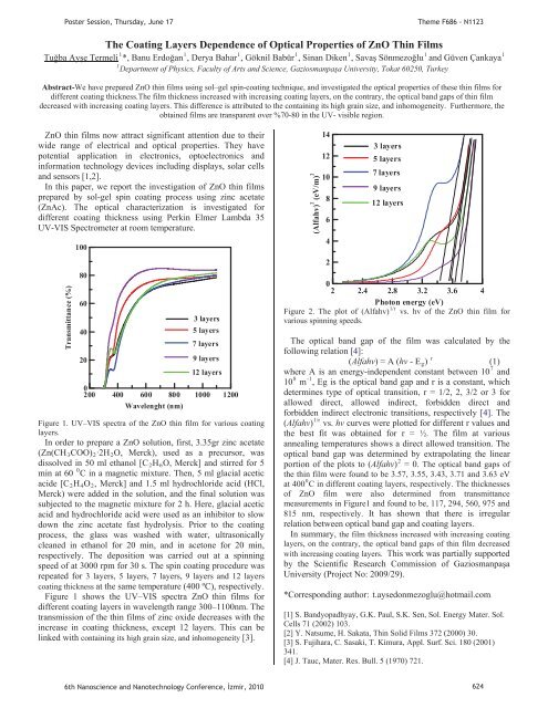
PP mPP vs.P vs.P =P (1)P andPoster Session, Thursday, June 17Theme F686 - N1123The Coat<strong>in</strong>g Layers Dependence of Optical Properties of ZnO Th<strong>in</strong> Films111111UTuba Aye TermeliUP P*, Banu ErdoanP P, Derya BaharP P, Göknil BabürP P, S<strong>in</strong>an DikenP P, Sava SönmezoluP Pand Güven ÇankayaP1PDepartment of Physics, Faculty of Arts and Science, Gaziosmanpaa University, Tokat 60250, TurkeyAbstract-We have prepared ZnO th<strong>in</strong> films us<strong>in</strong>g sol–gel sp<strong>in</strong>-coat<strong>in</strong>g technique, and <strong>in</strong>vestigated the optical properties of these th<strong>in</strong> films fordifferent coat<strong>in</strong>g thickness.The film thickness <strong>in</strong>creased with <strong>in</strong>creas<strong>in</strong>g coat<strong>in</strong>g layers, on the contrary, the optical band gaps of th<strong>in</strong> filmdecreased with <strong>in</strong>creas<strong>in</strong>g coat<strong>in</strong>g layers. This difference is attributed to the conta<strong>in</strong><strong>in</strong>g its high gra<strong>in</strong> size, and <strong>in</strong>homogeneity. Furthermore, theobta<strong>in</strong>ed films are transparent over %70-80 <strong>in</strong> the UV- visible region.1ZnO th<strong>in</strong> films now attract significant attention due to theirwide range of electrical and optical properties. They havepotential application <strong>in</strong> electronics, optoelectronics and<strong>in</strong>formation technology devices <strong>in</strong>clud<strong>in</strong>g displays, solar cellsand sensors [1,2].In this paper, we report the <strong>in</strong>vestigation of ZnO th<strong>in</strong> filmsprepared by sol-gel sp<strong>in</strong> coat<strong>in</strong>g process us<strong>in</strong>g z<strong>in</strong>c acetate(ZnAc). The optical characterization is <strong>in</strong>vestigated fordifferent coat<strong>in</strong>g thickness us<strong>in</strong>g Perk<strong>in</strong> Elmer Lambda 35UV-<strong>VI</strong>S Spectrometer at room temperature.Transmittance (%)100806040203 layers5 layers7 layers9 layers12 layers0200 400 600 800 1000 1200Wavelenght (nm)Figure 1. UV–<strong>VI</strong>S spectra of the ZnO th<strong>in</strong> film for various coat<strong>in</strong>glayers.In order to prepare a ZnO solution, first, 3.35gr z<strong>in</strong>c acetate(Zn(CHR3RCOO)R2R·2HR2RO, Merck), used as a precursor, wasdissolved <strong>in</strong> 50 ml ethanol [CR2RHR6RO, Merck] and stirred for 50m<strong>in</strong> at 60 P PC <strong>in</strong> a magnetic mixture. Then, 5 ml glacial aceticacide [CR2RHR4ROR2R, Merck] and 1.5 ml hydrochloride acid (HCl,Merck) were added <strong>in</strong> the solution, and the f<strong>in</strong>al solution wassubjected to the magnetic mixture for 2 h. Here, glacial aceticacid and hydrochloride acid were used as an <strong>in</strong>hibitor to slowdown the z<strong>in</strong>c acetate fast hydrolysis. Prior to the coat<strong>in</strong>gprocess, the glass was washed with water, ultrasonicallycleaned <strong>in</strong> ethanol for 20 m<strong>in</strong>, and <strong>in</strong> acetone for 20 m<strong>in</strong>,respectively. The deposition was carried out at a sp<strong>in</strong>n<strong>in</strong>gspeed of at 3000 rpm for 30 s. The sp<strong>in</strong> coat<strong>in</strong>g procedure wasrepeated for 3 layers, 5 layers, 7 layers, 9 layers and 12 layerscoat<strong>in</strong>g thickness at the same temperature (400 ºC), respectively.Figure 1 shows the UV–<strong>VI</strong>S spectra ZnO th<strong>in</strong> films fordifferent coat<strong>in</strong>g layers <strong>in</strong> wavelength range 300–1100nm. Thetransmission of the th<strong>in</strong> films of z<strong>in</strong>c oxide decreases with the<strong>in</strong>crease <strong>in</strong> coat<strong>in</strong>g thickness, except 12 layers. This can bel<strong>in</strong>ked with conta<strong>in</strong><strong>in</strong>g its high gra<strong>in</strong> size, and <strong>in</strong>homogeneity [3].(Alfahv) 2 (eV/m) 214121086423 layers5 layers7 layers9 layers12 layers02 2.4 2.8 3.2 3.6 4Photon energy (eV)1/rFigure 2. The plot of (Alfahv)P hv of the ZnO th<strong>in</strong> film forvarious sp<strong>in</strong>n<strong>in</strong>g speeds.The optical band gap of the film was calculated by thefollow<strong>in</strong>g relation [4]:r(Alfahv) = A (hv - ERgR) P7where A is an energy-<strong>in</strong>dependent constant between 10P8 -110PP, Eg is the optical band gap and r is a constant, whichdeterm<strong>in</strong>es type of optical transition, r = 1/2, 2, 3/2 or 3 forallowed direct, allowed <strong>in</strong>direct, forbidden direct andforbidden <strong>in</strong>direct electronic transitions, respectively [4]. The1/r(Alfahv)P hv curves were plotted for different r values andthe best fit was obta<strong>in</strong>ed for r = ½. The film at variousanneal<strong>in</strong>g temperatures shows a direct allowed transition. Theoptical band gap was determ<strong>in</strong>ed by extrapolat<strong>in</strong>g the l<strong>in</strong>ear2portion of the plots to (Alfahv)P 0. The optical band gaps ofthe th<strong>in</strong> film were found to be 3.57, 3.55, 3.43, 3.71 and 3.63 eV0at 400P PC <strong>in</strong> different coat<strong>in</strong>g layers, respectively. The thicknessesof ZnO film were also determ<strong>in</strong>ed from transmittancemeasurements <strong>in</strong> Figure1 and found to be, 117, 294, 560, 975 and815 nm, respectively. It has shown that there is irregularrelation between optical band gap and coat<strong>in</strong>g layers.In summary, the film thickness <strong>in</strong>creased with <strong>in</strong>creas<strong>in</strong>g coat<strong>in</strong>glayers, on the contrary, the optical band gaps of th<strong>in</strong> film decreasedwith <strong>in</strong>creas<strong>in</strong>g coat<strong>in</strong>g layers. This work was partially supportedby the Scientific Research Commission of GaziosmanpaaUniversity (Project No: 2009/29).*Correspond<strong>in</strong>g author: HTt.aysedonmezoglu@hotmail.comTH[1] S. Bandyopadhyay, G.K. Paul, S.K. Sen, Sol. Energy Mater. Sol.Cells 71 (2002) 103.[2] Y. Natsume, H. Sakata, Th<strong>in</strong> Solid Films 372 (2000) 30.[3] S. Fujihara, C. Sasaki, T. Kimura, Appl. Surf. Sci. 180 (2001)341.[4] J. Tauc, Mater. Res. Bull. 5 (1970) 721.6th Nanoscience and Nanotechnology Conference, zmir, 2010 624


