

Photonic crystals in biology - NanoTR-VI
Photonic crystals in biology - NanoTR-VI
Photonic crystals in biology - NanoTR-VI
- No tags were found...

Create successful ePaper yourself
Turn your PDF publications into a flip-book with our unique Google optimized e-Paper software.
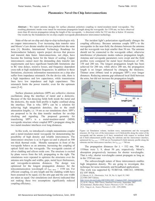
Poster Session, Thursday, June 17Theme F686 - N1123Plasmonics: Novel On-Chip InterconnectionsAbstract— We report antenna designs for surface plasmon polariton coupl<strong>in</strong>g to metal-<strong>in</strong>sulator-metal waveguides. Theresult<strong>in</strong>g plasmonic modes were tuned for maximum propagation length along the waveguide: for 1550 nm, we have observedmore than 40 micron propagation (along the length of the waveguide, +x direction) while for 532 nm this is below 10 micron.Our results lay the foundations for on-chip coupler-waveguide-photodetector <strong>in</strong>terconnect technology.State-of-the-art on-chip and chip-to-chip technologies relyon copper <strong>in</strong>terconnects. Ever <strong>in</strong>creas<strong>in</strong>g data transfer ratesand Moore’s Law dictate smaller devices packed <strong>in</strong>to the samearea [1]. Besides, International Technology Roadmap forSemiconductor Industry reports project devices that processand transmit data faster. Interconnections, not chips, havebecome the limit<strong>in</strong>g factor for the future of scal<strong>in</strong>g. Copper<strong>in</strong>terconnects cannot meet the demand<strong>in</strong>g data transfer raterequirements and have significant bandwidth limitations dueto RC time delays, resistive losses, and frequency dependentcross-talk at high modulation frequencies. In addition to theselimitations, electronic <strong>in</strong>formation transmission on a chip alsosuffer from impedance mismatch. On the device side, there isa high impedance and low capacitance, while transmissionl<strong>in</strong>es have low impedance and high capacitance. Thismismatch limits the power transfer, even for the optimumcases [2-4].The <strong>in</strong>cident light’s polarization significantly changes thecoupl<strong>in</strong>g efficiency. Because antennas couple SPP’s to thewaveguides <strong>in</strong> the near-field, the distance between the antennaand the waveguide was kept smaller than 50 nm. The antennashould not be connected to the waveguide either; otherwise<strong>in</strong>terference of plasmonic modes reduces propagation length.Antenna and waveguide parameters were swept and the fieldprofiles were compared for metal layer thicknesses of 100,150 and 200 nm. The longest propagation length has beenachieved for 200 nm, while above 200 nm, the propagationlength is no longer enhanced by chang<strong>in</strong>g the thickness.Th<strong>in</strong>ner arms (60nm) tend to propagate SPP’s over longerdistances. Reduc<strong>in</strong>g antenna gap enhanced local field betweenthe arms, but did not <strong>in</strong>crease the propagation length.Surface plasmon polaritons (SPP) are collective electronoscillations along the <strong>in</strong>terface of metal and a dielectric.Because of the fast decay<strong>in</strong>g fields both <strong>in</strong>side the metal andthe dielectric, the mode field profile is highly conf<strong>in</strong>ed alongthe <strong>in</strong>terface. That is why; SPP’s can be a solution forachiev<strong>in</strong>g high <strong>in</strong>tegration densities, due to the smallattenuation lengths, i.e. 14 nm as our simulations show. SPP’sare proposed to be the data transfer medium for on-chipclock<strong>in</strong>g and signal<strong>in</strong>g. The proposed geometry fortransferr<strong>in</strong>g SPP’s is a metal-<strong>in</strong>sulator-metal (MIM)waveguide structure where coupled SPP’s propagate along thetwo metal-<strong>in</strong>sulator <strong>in</strong>terfaces over long distances.In this work, we <strong>in</strong>troduced a simple nanoantenna couplerand a metal-<strong>in</strong>sulator-metal waveguide for demonstrat<strong>in</strong>g thepossibility of high density and reliable <strong>in</strong>terconnects. The<strong>in</strong>terconnect structure is as <strong>in</strong> Figure (a) and is placed on 500nm thick thermal oxide. Metallic nanoposts <strong>in</strong> front of thewaveguide behave as an antenna, <strong>in</strong>creas<strong>in</strong>g the coupl<strong>in</strong>g ofoptical field <strong>in</strong>to the waveguide. The waveguide consists ofsilver cladd<strong>in</strong>g and silicon oxide core. The structure is excitedby plane waves from the left, propagat<strong>in</strong>g to the right. Thesimulations were repeated to optimize the structures over theantenna arm lengths and widths, gaps, metal layer thicknesses,and waveguide-to-antenna distances. The design wasoptimized for the longest propagation distance for thetelecommunication wavelength of free space = 1550 nm. Forefficient coupl<strong>in</strong>g, (i) arm length and the cladd<strong>in</strong>g width havebeen assumed to be equal, (ii) the arm gap and the core widthare taken as equal. Our simulations (not shown) <strong>in</strong>dicated thatnot mak<strong>in</strong>g these two assumptions significantly reducedcoupl<strong>in</strong>g efficiency.Figure: (a) Simulation volume, <strong>in</strong>cident wave, nanoantenna and the waveguidestructure. (b) Top view of the <strong>in</strong>terconnect. (c) E-field profile along the center of thewaveguide and the antenna (y=0 l<strong>in</strong>e), normalized with respect to <strong>in</strong>cident field(d) E-field enhancement profile along the substrate and the <strong>in</strong>terconnect <strong>in</strong>terface,optimized for free space = 1550 nm (e) Normalized E-field <strong>in</strong>tensity profile along thesubstrate and the <strong>in</strong>terconnect <strong>in</strong>terface, for free space = 780 nm.The propagation distances for = 532 nm, 780 nm,1550nm were 3, 9, about 50 μm, respectively. Metal’sabsorption progressively <strong>in</strong>creases for shorter wavelengths.That is why; shorter wavelengths cannot propagate as long as<strong>in</strong> the 1550 nm case.The subwavelength nature of these <strong>in</strong>terconnects enableshigh <strong>in</strong>tegration density. We are go<strong>in</strong>g to <strong>in</strong>vestigate thistechnique for noise immunity and broadband applications.This work was supported by TUBITAK 108E163, 109E044,EU FP7 PIOS.[1] Moore, G. E., Electronics, Vol. 38, No. 8, April 19, 1965[2] ITRS 2007 Edition,http://www.itrs.net/L<strong>in</strong>ks/2007ITRS/2007_Chapters/2007_Interconnect.pdf[3] Ali K. Okyay, PhD Thesis, Stanford University, September 2007[4] Gramotnev, Bozhevolnyi; Nature <strong>Photonic</strong>s 4, 83 - 91 (2010)[5] L. Tang et. al., Nature <strong>Photonic</strong>s 2, 226 - 229 (2008)6th Nanoscience and Nanotechnology Conference, zmir, 2010 625


