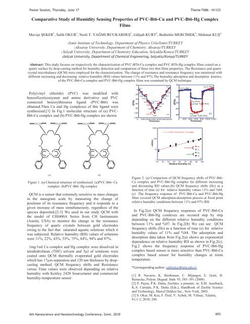
Poster Session, Thursday, June 17Theme F686 - N1123Comparative Study of Humidity Sens<strong>in</strong>g Properties of PVC-Bt6-Cu and PVC-Bt6-Hg ComplexFilmsMavişe ŞEKER 1 , Salih OKUR 1 , Nesli T. YAĞMURCUKARDEŞ 1 , Gülşah KURT 2 , Bedrett<strong>in</strong> MERCİMEK 3 , Mahmut KUŞ 41Izmir Institute of Technology, Department of Physics Urla/Izmir/TURKEY2Aksaray University, Department of Chemistry, Aksaray/TURKEY3 Selçuk University, Department of Chemistry Education, Selçuklu/Konya/TURKEY4Selçuk University, Department of Chemical Eng<strong>in</strong>eer<strong>in</strong>g, Selçuklu/Konya/TURKEYAbstract: This study focuses on respectively the characterization of PVC-BT6-Cu complex and PVC-BT6-Hg complex films coated on aquartz surface by drop-cast<strong>in</strong>g method for humidity detection and comparison of these two th<strong>in</strong> films properties. The Resistance and quartzcrystal microbalance (QCM) were employed for the characterization. The change of resistance and resonance frequency was monitored withdifferent <strong>in</strong>creas<strong>in</strong>g and decreas<strong>in</strong>g relative humidity (RH) values between 11% and 97%.The humidity adsorption and desorption k<strong>in</strong>eticsof the PVC-Bt6-Cu complex and PVC-Bt6-Hg complex films was exam<strong>in</strong>ed by QCM technique.Poly(v<strong>in</strong>yl chloride) (PVC) was modified withbenzoilizotiyosiyanat and am<strong>in</strong>e derivative and PVCconnected benzoylthiourea ligand (PVC-Bt6) wasobta<strong>in</strong>ed.Then Cu and Hg complexes of this ligand weresynthesized.[1] In Fig.1 molecular structure of (a) PVC-Bt6-Cu complex and (b) PVC-Bt6-Hg complex are shown.CH 2 -CHCH 2 -CHCH 2 -CHCH 2 -CH2020%11%11 RH%11%11 RH00%22%22-20%43%43-20-40 %53%53-60%75Cu-PVCCu-PVC-40%75(under %84 RH)%84%84-80%94-60%94-100Hg-PVC (a) -80Hg-PVC (b)%97(under %84 RH)-120200 400 600 800 1000 1200Time/sec0 1000 2000 3000 4000 5000 6000Time/sec0dF/Hz1000dF/HzNNNNy = 4.1948 * e^(0.032107x) R= 0.98952100HNNSOCuSONHNHNNSOHgSONHN- f(Hz)Hgdownward10CuHgupwardCu(c)120 30 40 50 60 70 80 90 100Relative Humidity (%)(a)Figure 1. (a) Chemical structure of synthesized (a)PVC-Bt6- Cucomplex (b)PVC-Bt6- Hg complexQCM is a sensor that extremely sensitive to mass changes<strong>in</strong> the nanogram scale by measur<strong>in</strong>g the change ofpositions of its resonance frequency and it responds to agiven <strong>in</strong>crease of mass simultaneously, regardless of thespecies deposited.[2-3] We used <strong>in</strong> our study QCM withthe model of CHI400A Series from CH Instruments(Aust<strong>in</strong>, USA) to monitor the change <strong>in</strong> the resonancefrequency of quartz <strong>crystals</strong> between gold electrodesow<strong>in</strong>g to the fact that saturated aquatic solutions which itwas subjected. Relative humidity (RH) values of solutionswere 11%, 22%, 43%, 53%, 75%, 84%, 94% and 97%.1mg/1ml Cu complex and Hg complex were dissolved <strong>in</strong>tetrahidrofuran (THF) solvent and 5μl of solutions werecoated onto QCM thermally evaporated gold electrodeswhich has 17μm separation and 120 nm thickness by dropcast<strong>in</strong>gmethod. QCM frequency shifts and Resistanceversus Time values were observed depend<strong>in</strong>g on relativehumidity with Keitley 2420 Sourcemeter and commercialhumidity-temperature sensor.(b)Figure 2. (a) Comparison of QCM frequency shifts of PVC-Bt6-Cu complex and PVC-Bt6-Hg complex for different <strong>in</strong>creas<strong>in</strong>gand decreas<strong>in</strong>g RH values.(b) QCM frequency shifts (Hz) as afunction of time (s) for relative humidity values 11% and %84.(c) The frequency response of PVC-Bt6-Cu and PVC-Bt6-Hgfilms covered QCM adsorption-desorption process at fixed po<strong>in</strong>trelative humidity conditions between 11% and 97% RH.In Fig.2(a) QCM frequency responses of PVC-Bt6-Cuand PVC-Bt6-Hg comlexes are occured step by stepdepend<strong>in</strong>g on the different relative humidity conditionsbetween 11% and %97. In Fig.2(b) We can see QCMfrequency shifts (Hz) as a function of time (s) for relativehumidity values of 11% and %84. The adsorption anddesorption data taken from Fig.2(a) shows an exponentialdependence on relative humidity RH as shown <strong>in</strong> Fig.2(c).Fig.2 shows the frequency response of PVC-Bt6-Hgcomplex based sensor is more sensitive than PVC-Bt6-Cucomplex based sensor for humidity changes at roomtemperature.*Correspond<strong>in</strong>g author: salihokur@iyte.edu.tr[1] R. Navarro, K. Bierbrauer, C. Mijangos, E. Goiti, H.Re<strong>in</strong>ecke, Polym. Degrad. Stab. 93, 585–591 (2008)[2] P. Payra, P.K. Dutta, Zeolites: a premier, <strong>in</strong>: S.M. Auerbach,K.A. Carrado, P.K. Dutta (Eds.), Handbook of Zeolite Scienceand Technology, Marcel Dekker Inc., New York, 2003.[3] S. Okur, M. Kus, F. Özel, V. Aybek, M. Yilmaz, Talanta,81;1-2; 2010; 248.6th Nanoscience and Nanotechnology Conference, zmir, 2010 693
Poster Session, Thursday, June 17Theme F686 - N1123Fabrication of Micro Channels with Angled Sidewall on Silicon by Nd:YAG Laser AblationAlperen Acemoglu, 1 Veysel Ozkapici 2,* ,Vural Kara 1 ,Omid Tayafeh 3 ,Husey<strong>in</strong> Kizil 4 and Levent Trabzon 1,*1 Department of Mechanical Eng<strong>in</strong>eer<strong>in</strong>g, Istanbul Technical University, Gumussuyu, Istanbul 34437, Turkey2 BNM Fabrika Biyo Nano Mikro Tek. San. Ve Tic. Ek<strong>in</strong>ciler Cad. 7/4 stanbul 34830, Turkey3 Department of Electronics and Communication Eng<strong>in</strong>eer<strong>in</strong>g, Istanbul Technical University, Maslak, Istanbul 34469, Turkey4 Department of Metallurgical and Materials Eng<strong>in</strong>eer<strong>in</strong>g, Istanbul Technical University, Maslak, Istanbul 34469, TurkeyAbstract— We present experimental results on microfabrication of micro channels with angled sidewall on silicon surface by Nd:YAG laser.The purpose is to create V-shaped deep micro channels on silicon surface for produc<strong>in</strong>g nano-sharp micro Si-knife. The results can be used tocharacterize the behavior of ablation process under different laser parameters to achieve optimal process<strong>in</strong>g conditions for Si-micromicromach<strong>in</strong>g<strong>in</strong> MEMS such as V-shaped channels, slots and s<strong>in</strong>gulation process of vias.Micro channels on silicon wafer play an important role <strong>in</strong>many MEMS and NEMS applications. There are severalmicrofabrication processes for creat<strong>in</strong>g proper micro channelson silicon surface. Conventional chemical and mechanicalprocesses like etch<strong>in</strong>g, engrav<strong>in</strong>g and saw<strong>in</strong>g have beensuccessfully applied on to fabrication of micro channels [1, 2].Although well developed and mature production process, theyare not suitable for all k<strong>in</strong>d of MEMS application. That’s whylaser are widely used to create this k<strong>in</strong>d of channels onmaterial, laser fabrication process is a non contact processtherefore preferred <strong>in</strong> our task.Lasers are a powerful tool for micromach<strong>in</strong><strong>in</strong>gapplications. A focused laser beam can easily be concentratedonto a small target of a few micron diameters. The lasermaterial-<strong>in</strong>teraction <strong>in</strong> this target area will be controlled bylaser parameters such as wavelength, pulse energy and pulseduration which determ<strong>in</strong>e peak power density [3]. Certa<strong>in</strong> setsof parameters can cause thermal effects for mark<strong>in</strong>g, cutt<strong>in</strong>g,and drill<strong>in</strong>g.In our work, we have specially chosen to work withNd:YAG DPSS laser which has 1064 nm wavelength and 60W maximum power. There were limited survey on that, mostof the laser on literature was <strong>in</strong> the UV range with eitherfemto- or pico-seconds system, which are very expensive. Ourma<strong>in</strong> focus was creat<strong>in</strong>g those micro channels by nanosecondlaser with a wavelength of 1064 nm.One of the important f<strong>in</strong>d<strong>in</strong>gs <strong>in</strong> the study is to have U-shaped channels with laser beam directed on the Si-waferperpendicular. This observation is def<strong>in</strong>ed as taper<strong>in</strong>g affectand it depends on the repletion of the laser ablation and depthof the channel produced <strong>in</strong> the ablation process [5]. Taper<strong>in</strong>gaffect is around 30°- 40° for 10 – 50 μm deep channels andthey are roughly V-shaped channel as shown <strong>in</strong> Fig. 2a.Taper<strong>in</strong>g affect was reduced to 10 °- 15° when channel depthis <strong>in</strong> between 51 and 150 μm.Ma<strong>in</strong> aim of this work is to create angled sidewallproduction on silicon wafer by laser. Then, we exam<strong>in</strong>ed laserbeam ablation on Si-wafer by different angles with laser beam.By means of adjustable wedge, the Si is oriented as 30°-45°-60° degree with respect to <strong>in</strong>com<strong>in</strong>g laser <strong>in</strong> order to seesidewall affect and channel-wall angles. The channel-wallangles should be 30°-45°-60° degrees after <strong>in</strong>cl<strong>in</strong>ed Si-waferablation by laser if there is no taper<strong>in</strong>g effect. We measuredchannel-wall angles by profilometer on each Si wafer ablatedby a different angle. We found that the channel-wall angles are38°-42°, 29°-34° and 19°-22° for ideally expected sidewallangel 60°, 45° and 30°, respectively. The difference betweenmeasured and expected angles is due to taper<strong>in</strong>g effect <strong>in</strong> Silaser ablation.(a)(b)Figure 1: (a) Schematic draw<strong>in</strong>gs of angled channels set up (b) Angledmicro channel fabrication setup.We first studied ablation effect of perpendicular laserbeam on silicon surface. We observe and measure the effect oflaser on scribed or grooved channels by profilometre bychang<strong>in</strong>g laser ablation velocity, frequency, power andrepetition. It is been showed that 40 – 100 μm wide and 5- 250μm deep groves can easily been produced by laser. There werebig debris or (HAZ) around the channel due to thermal affectof laser. As our expectation and previous literature <strong>in</strong>fo,ablation affect of laser <strong>in</strong>creased by power, frequency,repetition <strong>in</strong>crements and velocity decrements [3]. The degreeof ablation does not l<strong>in</strong>early depend on the aforementionedparameters; the relationship is very complex and wellexpla<strong>in</strong>ed [4].Figure 2: (a) Optical microscope picture of micro channels produced by laser(b) Profilometre result graph of sidewall angel of laser ablated micro channel.This work was partially supported by TUBITAK under Grant No. 8080090*Correspond<strong>in</strong>g authors: levent.trabzon@itu.edu.tr andveysel.ozkapici@bnmfabric.com[1] G.S. May,S.M.Sze, Fundamentals of semiconductor fabrication,JonhWilley & Sons, Inc.,(2004).[2] G. T. A. Kovacks, N. Maluf,G.W. Crabtree,Bulk Micromach<strong>in</strong><strong>in</strong>g ofSilicon K. Petersen, IEEE, VOL. 86, NO. 8, (1998)Phys. Today 57, No. 12, 39 (2004).[3]A. Ostendorf, K. Koerber, T. Nether, T. Temme: “Material Process<strong>in</strong>gApplications for Diode Pumped Solid State Lasers” In: Lambda Highlights,No. 57 , Gött<strong>in</strong>gen (2000)[4] Holmes A.S., Pedder J.E.A., Boehlen K., Advanced laser micromach<strong>in</strong><strong>in</strong>gprocesses for MEMS applications, SPIE Proceed<strong>in</strong>gs Vol. 6261,(2006)[5] T. Otani,L. Herbst, M.Hegl<strong>in</strong>g.S.V.Govorkov, A.O. WiessnerMicrodrill<strong>in</strong>g and micromach<strong>in</strong><strong>in</strong>g with diode-pumped solid-state lasersBogdanovic et al., Appl. Phys. A 79, 1335–1339 (2004) (2003).6th Nanoscience and Nanotechnology Conference, zmir, 2010 694
- Page 1:
Poster Presentations3rd Day17 June
- Page 4 and 5:
Determination of Dielectric Anisotr
- Page 7 and 8:
Poster Session, Thursday, June 17Th
- Page 9 and 10:
PP mPP vs.P =P,PP (1)P andPoster Se
- Page 11 and 12:
PP mPP vs.P =P,PP (1)P andPoster Se
- Page 13 and 14:
PP andPoster Session, Thursday, Jun
- Page 15 and 16:
Poster Session, Thursday, June 17Th
- Page 17 and 18:
PP and770 772 774 776 778 780 782 7
- Page 19 and 20:
Poster Session, Thursday, June 17Th
- Page 21 and 22:
Poster Session, Thursday, June 17Th
- Page 23 and 24:
P25,Poster Session, Thursday, June
- Page 25 and 26:
PP TOBBPoster Session, Thursday, Ju
- Page 27 and 28:
PisPPisisisP,PisPoster Session, Thu
- Page 29 and 30:
U NeslihanPPPPoster Session, Thursd
- Page 31 and 32:
Poster Session, Thursday, June 17Th
- Page 33 and 34: PPPoster Session, Thursday, June 17
- Page 35 and 36: PPoster Session, Thursday, June 17T
- Page 37 and 38: P onP viaPP wereP upPoster Session,
- Page 39 and 40: P ·cm.PVPPPsPPPPP andPoster Sessio
- Page 41 and 42: Poster Session, Thursday, June 17Th
- Page 43 and 44: PPoster Session, Thursday, June 17T
- Page 45 and 46: PPoster Session, Thursday, June 17T
- Page 47 and 48: Poster Session, Thursday, June 17Th
- Page 49 and 50: PErkanPoster Session, Thursday, Jun
- Page 51 and 52: Poster Session, Thursday, June 17Th
- Page 53 and 54: Poster Session, Thursday, June 17Th
- Page 55 and 56: PPPP andPoster Session, Thursday, J
- Page 57 and 58: Poster Session, Thursday, June 17Th
- Page 59 and 60: Poster Session, Thursday, June 17Th
- Page 61 and 62: T PeptideTPP,PP,PP andTT2429TTTTTT
- Page 63 and 64: Poster Session, Thursday, June 17Th
- Page 65 and 66: PPoster Session, Thursday, June 17T
- Page 67 and 68: Poster Session, Thursday, June 17Th
- Page 69 and 70: PPPoster Session, Thursday, June 17
- Page 71 and 72: Poster Session, Thursday, June 17Th
- Page 73 and 74: Poster Session, Thursday, June 17Th
- Page 75 and 76: PT AdditionalT ThePoster Session, T
- Page 77 and 78: Poster Session, Thursday, June 17Th
- Page 79 and 80: Poster Session, Thursday, June 17Th
- Page 81 and 82: Poster Session, Thursday, June 17Th
- Page 83: PPoster Session, Thursday, June 17T
- Page 87 and 88: PPPoster Session, Thursday, June 17
- Page 89 and 90: Poster Session, Thursday, June 17Hu
- Page 91 and 92: Poster Session, Thursday, June 17Th
- Page 93 and 94: PPPPPPoster Session, Thursday, June
- Page 95 and 96: Poster Session, Thursday, June 17Th
- Page 97 and 98: Poster Session, Thursday, June 17Th
- Page 99 and 100: Poster Session, Thursday, June 17Th
- Page 101 and 102: PPoster Session, Thursday, June 17T
- Page 103 and 104: Poster Session, Thursday, June 17Th
- Page 105 and 106: PPPPPPPoster Session, Thursday, Jun
- Page 107 and 108: Poster Session, Thursday, June 17Th
- Page 109 and 110: PPPR2R PIN(80)PPgPP OzlemPPoster Se
- Page 111 and 112: Poster Session, Thursday, June 17Th
- Page 113 and 114: Poster Session, Thursday, June 17Th
- Page 115 and 116: P onPP toP coordinatedPPoster Sessi
- Page 117 and 118: PPPPP,PP,P(PR RmPoster Session, Thu
- Page 119 and 120: Poster Session, Thursday, June 17Th
- Page 121 and 122: Poster Session, Thursday, June 17Th
- Page 123 and 124: PP InstitutePP DepartmentPoster Ses
- Page 125 and 126: andPCPPoster Session, Thursday, Jun
- Page 127 and 128: PP scatteringPYusufPP Corresponding
- Page 129 and 130: PP toPoster Session, Thursday, June
- Page 131 and 132: PP andPoster Session, Thursday, Jun
- Page 133 and 134: PPPPoster Session, Thursday, June 1
- Page 135 and 136:
PPoster Session, Thursday, June 17T
- Page 137 and 138:
PPP andP (.cm).Poster Session, Thur
- Page 139 and 140:
PP tiltP andP editionPoster Session
- Page 141 and 142:
PP andPPoster Session, Thursday, Ju
- Page 143 and 144:
Poster Session, Thursday, June 17Th
- Page 145 and 146:
PP forP forP edit.PPoster Session,
- Page 147 and 148:
Poster Session, Thursday, June 17Th
- Page 149 and 150:
Poster Session, Thursday, June 17Th
- Page 151 and 152:
PP ionicPP ,PPoster Session, Thursd
- Page 153 and 154:
PP lightPoster Session, Thursday, J
- Page 155 and 156:
Poster Session, Thursday, June 17Th
- Page 157 and 158:
PPoster Session, Thursday, June 17T
- Page 159 and 160:
Poster Session, Thursday, June 17Th
- Page 161 and 162:
PandPoster Session, Thursday, June
- Page 163 and 164:
Poster Session, Thursday, June 17 T
- Page 165 and 166:
PPPoster Session, Thursday, June 17
- Page 167 and 168:
PPoster Session, Thursday, June 17T
- Page 169 and 170:
PPoster Session, Thursday, June 17T
- Page 171 and 172:
PPoster Session, Thursday, June 17T
- Page 173 and 174:
PP DepartmentNanoscienceTPPoster Se
- Page 175 and 176:
Poster Session, Thursday, June 17Th
- Page 177 and 178:
Poster Session, Thursday, June 17Th
- Page 179 and 180:
PPPoster Session, Thursday, June 17
- Page 181 and 182:
PPPPPoster Session, Thursday, June
- Page 183 and 184:
PPPPoster Session, Thursday, June 1
- Page 185 and 186:
PPoster Session, Thursday, June 17T
- Page 187 and 188:
PPoster Session, Thursday, June 17T
- Page 189 and 190:
PPoster Session, Thursday, June 17T
- Page 191 and 192:
Poster Session, Thursday, June 17Th
- Page 193 and 194:
Poster Session, Thursday, June 17Th
- Page 195 and 196:
0T0T0T0T AsPPPP werePoster Session,
- Page 197 and 198:
PPoster Session, Thursday, June 17T
- Page 199 and 200:
PPPPPoster Session, Thursday, June
- Page 201 and 202:
PPoster Session, Thursday, June 17T
- Page 203 and 204:
PPoster Session, Thursday, June 17T
- Page 205 and 206:
Poster Session, Thursday, June 17Th
- Page 207 and 208:
PPoster Session, Thursday, June 17T
- Page 209 and 210:
PPoster Session, Thursday, June 17T
- Page 211:
Poster Session, Thursday, June 17AF