

Photonic crystals in biology - NanoTR-VI
Photonic crystals in biology - NanoTR-VI
Photonic crystals in biology - NanoTR-VI
- No tags were found...

Create successful ePaper yourself
Turn your PDF publications into a flip-book with our unique Google optimized e-Paper software.
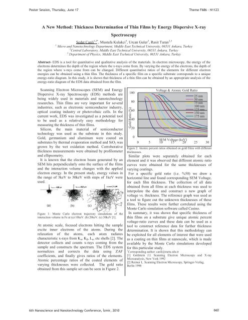
Poster Session, Thursday, June 17Theme F686 - N1123A New Method: Thickness Determ<strong>in</strong>ation of Th<strong>in</strong> Films by Energy Dispersive X-raySpectroscopySedat Canli 1,2* , Mustafa Kulakci 3 , Urcan Guler 3 , Rasit Turan 2,31 Micro and Nanotechnology Department, Middle East Technical University, 06531 Ankara, Turkey2 Central Laboratory, Middle East Technical University, 06531 Ankara, Turkey3 Department of Physics, Middle East Technical University, 06531 Ankara, TurkeyAbstract- EDS is a tool for quantitative and qualitative analysis of the materials. In electron microscopy, the energy of theelectrons determ<strong>in</strong>es the depth of the region where the x-rays come from. By vary<strong>in</strong>g the energy of the electrons, the depth ofthe region where x-rays come from can be changed. Different quantitative ratios of the elements for different electronenergies can be obta<strong>in</strong>ed us<strong>in</strong>g a th<strong>in</strong> film. The thickness of a specific film on a specific substrate corresponds to a uniqueenergy-ratio diagram. In this study, it is shown that thickness of a th<strong>in</strong> film can be obta<strong>in</strong>ed by an appropriate analysis of theenergy-ratio diagram of the EDS data obta<strong>in</strong>ed from the film.Scann<strong>in</strong>g Electron Microscopes (SEM) and EnergyDispersive X-ray Spectroscopy (EDS) methods arebe<strong>in</strong>g widely used <strong>in</strong> materials and nanotechnologyresearches. Th<strong>in</strong> films are very important for several<strong>in</strong>dustries, such as electronic semiconductor <strong>in</strong>dustry,optical coat<strong>in</strong>g <strong>in</strong>dustry or photovoltaic cells. In thecurrent work, EDS was <strong>in</strong>vestigated as a potential toolto be used as a relatively easy methodology formeasur<strong>in</strong>g the thickness of th<strong>in</strong> films.Silicon, the ma<strong>in</strong> material of semiconductortechnology was used as the substrate <strong>in</strong> this study.Gold, germanium and alum<strong>in</strong>um were coated onsubstrates by thermal evaporation method and SiO 2 wasgrown by the wet oxidation method. Corroborativethickness measurements were obta<strong>in</strong>ed by profilometerand ellipsometry.It is known that the electron beam generated by anSEM hits perpendicularly onto the surface of the filmsand the <strong>in</strong>teraction volume changes with the appliedelectron energy. In the present study, energy values <strong>in</strong>the range of 3keV to 30keV with steps of 1keV wereused.Figure 1: Monte Carlo electron trajectory simulations of the<strong>in</strong>teraction volume <strong>in</strong> Fe at (a) 10keV. (b) 20keV. (c) 30keV [1].At atomic scale, focused electrons hitt<strong>in</strong>g the sampleexcite <strong>in</strong>ner electrons of the atoms. Dur<strong>in</strong>g therelaxation of the atoms, each atom radiatescharacteristic x-rays from K α , K β , L α , etc shells [2]. Thedetector collects and counts x-rays com<strong>in</strong>g from thesample and constructs the spectrum. The EDS systemnormalizes and corrects the data us<strong>in</strong>g ZAFcoefficients, and f<strong>in</strong>ally gives ratios of the elements.Atomic percentage ratios of the coated elements ofvary<strong>in</strong>g thicknesses were collected. The gold ratioobta<strong>in</strong>ed from this sample set can be seen <strong>in</strong> Figure 2.Gold Ratio (%)100806040200Voltage & Atomic Gold Ratio25 nm50 nm75 nm100 nm125 nm150 nm175 nmSEM Voltage (keV)0 5 10 15 20 25 30Figure 2: Atomic percent ratios obta<strong>in</strong>ed on gold films with differentthicknesses.Similar plots were separately obta<strong>in</strong>ed for eachelement and it was observed that different atomic ratiocurves were obta<strong>in</strong>ed for the same thicknesses ofvary<strong>in</strong>g coat<strong>in</strong>gs.For a specific gold ratio (i.e. %50) we draw ahorizontal l<strong>in</strong>e and found correspond<strong>in</strong>g SEM Voltage,for each film thickness. The collection of all dataobta<strong>in</strong>ed from all films at each thickness was used to<strong>in</strong>terpolate the data and construct a new graph ofvoltage vs. thickness. The reference graph was used asa tool to figure out the unknown thicknesses of thesefilms. These results were further correlated us<strong>in</strong>g theMonte Carlo simulation software called Cas<strong>in</strong>o.In summary, it was shown that specific thickness ofth<strong>in</strong> films on a substrate give unique atomic percentvoltage-ratio curves and these data can be used as atool to construct reference data for further thicknessdeterm<strong>in</strong>ation. It is shown that this methodology canbe exploited for all elements of <strong>in</strong>terest that were usedas a coat<strong>in</strong>g on th<strong>in</strong> films at nanoscale, which is madeavailable by the Monte Carlo simulations developedfor this particular study.* Correspond<strong>in</strong>g author: canli@metu.edu.tr[1] Goldste<strong>in</strong> J.I. Scann<strong>in</strong>g Electron Microscopy and X-rayMicroanalysis, New York 1992[2] Reimer L. Scann<strong>in</strong>g Electron Microscopy, Spr<strong>in</strong>ger-Verlag,Berl<strong>in</strong> 19986th Nanoscience and Nanotechnology Conference, zmir, 2010 660


