

Photonic crystals in biology - NanoTR-VI
Photonic crystals in biology - NanoTR-VI
Photonic crystals in biology - NanoTR-VI
- No tags were found...

You also want an ePaper? Increase the reach of your titles
YUMPU automatically turns print PDFs into web optimized ePapers that Google loves.
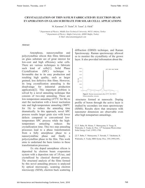
Poster Session, Thursday, June 17Theme F686 - N1123CRYSTALLIZATION OF THIN Si FILM FABRICATED BY ELECTRON BEAMEVAPORATION ON GLASS SUBSTRATE FOR SOLAR CELLL APPLICATIONSM. Karaman a , Ö. Tüzün b , R. Turan a , . Oktik ba Department of Physics, Middle East Technical University, 06531 Ankara, Turkeyb Department of Physics, Mula University, 48000 Mula, TurkeyE-Mail: mkaramanm@gmail.comAbstractAmorphous, nanocrystall<strong>in</strong>e andpolycrystall<strong>in</strong>e silicon th<strong>in</strong> films fabricatedon glass substrate are of great <strong>in</strong>terest forlow-cost and high efficiency solar cells.There are various techniques to fabricatesuch k<strong>in</strong>d of cells[1]. Solid PhaseCrystallization (SPC) technique isfavourable due to its easy production andresult<strong>in</strong>g high quality, such as largergra<strong>in</strong>ed, less defective th<strong>in</strong> films. However,its long crystallization anneal<strong>in</strong>g is thedisadvatage for <strong>in</strong>dustrial productionapplication[2]. This important problem issolved by a novel anneal<strong>in</strong>g technique thatconsists of two-step anneal<strong>in</strong>g. These arelow-temperature anneal<strong>in</strong>g (475 o C for 8h) tostart the nucleation with a lower nucleationrate and high-temperature anneal<strong>in</strong>g (900 o Cfor 1h) to reduce the anneal<strong>in</strong>g timedramatically. In this approach, novel SPCprocess results larger gra<strong>in</strong> size with lowerdefects compared to conventional lowtemperatureSPC process while the hightemperatureanneal<strong>in</strong>g reduces thecrystallization time. This two step anneal<strong>in</strong>gprocesses lead to a phase transformationfrom a fully amorphous phase to ananocrystall<strong>in</strong>e phase and f<strong>in</strong>ally apolycrystall<strong>in</strong>e phase <strong>in</strong> the film. This workaims to undertand the basic k<strong>in</strong>tics <strong>in</strong> thesetransformation processes.Ex situ doped amorphous silicon isdeposited by electron beam evaporationsystem with a depositon rate of 3Å/sec, andcrystallized by classical thermal process.The structural analysis of the films formedby this novel anneal<strong>in</strong>g process is analyzedby optical microscopy, scann<strong>in</strong>g electronmicroscopy (SEM), electron back scatter<strong>in</strong>gdiffraction (EBSD) technique, and RamanSpectroscopy. Raman spectroscopy allowedus to monitor the crystall<strong>in</strong>ity of the grownlayer. It also provided <strong>in</strong>fromation about theFigure1. Raman measurement after 475°C 8h+900°C60m<strong>in</strong> anneal<strong>in</strong>g processstructures formed at nanoscale. Dop<strong>in</strong>gprofile of boron through the active layer isstudied by secondary ion mass spectroscopy(SIMS). Results show that structures withnanometer dimension are observable evenafter high temeparture anneal<strong>in</strong>gs.[1] T. Baba, M. Shima, T. Matsuyama, S. Tsuge, K.Wakisaka, S. Tsuda, In: Proc. 13 th European PhotovoltaicSolar Energy Conf. (1995) 1708.[2] T. Baba, T. Matsuyama, T. Sawada, T. Takahama, K.Wakisaka, S. Tsuda, MRS Symp. Proc. 358 (1995) 8956th Nanoscience and Nanotechnology Conference, zmir, 2010 768


