Photonic crystals in biology - NanoTR-VI
Photonic crystals in biology - NanoTR-VI
Photonic crystals in biology - NanoTR-VI
- No tags were found...
Create successful ePaper yourself
Turn your PDF publications into a flip-book with our unique Google optimized e-Paper software.
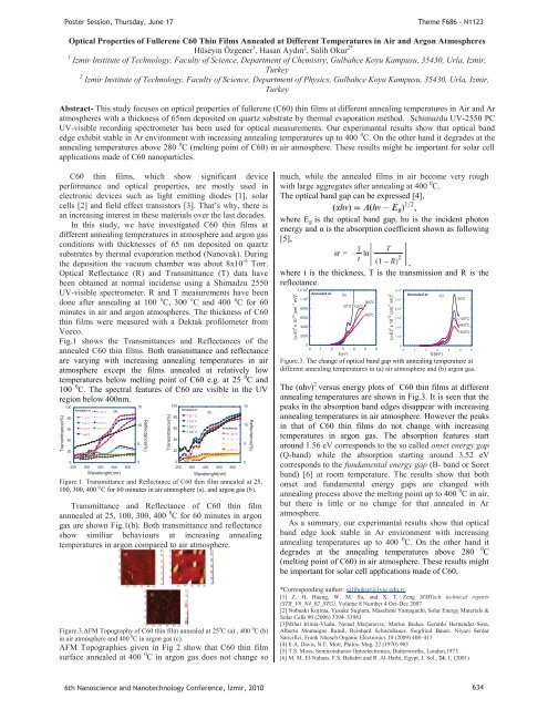
Poster Session, Thursday, June 17Theme F686 - N1123Optical Properties of Fullerene C60 Th<strong>in</strong> Films Annealed at Different Temperatures <strong>in</strong> Air and Argon AtmospheresHüsey<strong>in</strong> Özgener 1 , Hasan Aydın 2 , Salih Okur 2*1 Izmir Institute of Technology, Faculty of Science, Department of Chemistry, Gulbahce Koyu Kampusu, 35430, Urla, Izmir,Turkey2 Izmir Institute of Technology, Faculty of Science, Department of Physics, Gulbahce Koyu Kampusu, 35430, Urla, Izmir,TurkeyAbstract- This study focuses on optical properties of fullerene (C60) th<strong>in</strong> films at different anneal<strong>in</strong>g temperatures <strong>in</strong> Air and Aratmospheres with a thickness of 65nm deposited on quartz substrate by thermal evaporation method. Schimazdu UV-2550 PCUV-visible record<strong>in</strong>g spectrometer has been used for optical measurements. Our experimantal results show that optical bandedge exhibit stable <strong>in</strong> Ar environment with <strong>in</strong>creas<strong>in</strong>g anneal<strong>in</strong>g temperatures up to 400 0 C. On the other hand it degrades at theanneal<strong>in</strong>g temperatures above 280 0 C (melt<strong>in</strong>g po<strong>in</strong>t of C60) <strong>in</strong> air atmosphere. These results might be important for solar cellapplications made of C60 nanoparticles.C60 th<strong>in</strong> films, which show significant deviceperformance and optical properties, are mostly used <strong>in</strong>electronic devices such as light emitt<strong>in</strong>g diodes [1], solarcells [2] and field effect transistors [3]. That’s why, there isan <strong>in</strong>creas<strong>in</strong>g <strong>in</strong>terest <strong>in</strong> these materials over the last decades.In this study, we have <strong>in</strong>vestigated C60 th<strong>in</strong> films atdifferent anneal<strong>in</strong>g temperatures <strong>in</strong> atmosphere and argon gasconditions with thicknesses of 65 nm deposited on quartzsubstrates by thermal evaporation method (Nanovak). Dur<strong>in</strong>gthe deposition the vacuum chamber was about 8x10 -6 Torr.Optical Reflectance (R) and Transmittance (T) data havebeen obta<strong>in</strong>ed at normal <strong>in</strong>cidense us<strong>in</strong>g a Shimadzu 2550UV-visible spectrometer. R and T measurements have beendone after anneal<strong>in</strong>g at 100 o C, 300 o C and 400 o C for 60m<strong>in</strong>utes <strong>in</strong> air and argon atmospheres. The thickness of C60th<strong>in</strong> films were measured with a Dektak profilometer fromVeeco.Fig.1 shows the Transmittances and Reflectances of theannealed C60 th<strong>in</strong> films. Both transmittance and reflectanceare vary<strong>in</strong>g with <strong>in</strong>creas<strong>in</strong>g anneal<strong>in</strong>g temperatures <strong>in</strong> airatmosphere except the films annealed at relatively lowtemperatures below melt<strong>in</strong>g po<strong>in</strong>t of C60 e.g. at 25 0 C and100 0 C. The spectral features of C60 are visible <strong>in</strong> the UVregion below 400nm.Transmittance(%)10080604020Annealed atT 25 0 CT 100 o CT 300 0 CT 400 0 CR 25 0 CR 100 0 CR 300 0 CR 400 0 C(a)0200 300 400 500 600Wavelenght(nm)151050Reflectance(%)Transmittance(%)10080604020Annealed atT 250 CT 100 0 CT 300 0 CT 400 0 C(b)R 25 0 CR 100 0 CR 300 0 CR 400 0 C0200 300 400 500 600Wavelenght(nm)Annealed atFigure.1. Transmittance and Reflectance of C60 th<strong>in</strong> film annealed at 25,100, 300, 400 O C for 60 m<strong>in</strong>utes <strong>in</strong> air atmosphere (a), and argon gas (b).Transmittance and Reflectance of C60 th<strong>in</strong> filmannnealed at 25, 100, 300, 400 0 C for 60 m<strong>in</strong>utes <strong>in</strong> argongas are shown Fig.1(b). Both transmittance and reflectanceshow similiar behaviours at <strong>in</strong>creas<strong>in</strong>g anneal<strong>in</strong>gtemperatures <strong>in</strong> argon compared to air atmosphere.Figure.3.AFM Topography of C60 th<strong>in</strong> film annealed at 25 0 C (a) , 400 0 C (b)<strong>in</strong> air atmosphere and 400 0 C <strong>in</strong> argon gas (c).AFM Topographies given <strong>in</strong> Fig 2 show that C60 th<strong>in</strong> filmsurface annealed at 400 0 C <strong>in</strong> argon gas does not change so151050Reflectance(%)much, while the annealed films <strong>in</strong> air become very roughwith large aggregates after anneal<strong>in</strong>g at 400 0 C.The optical band gap can be expressed [4],where E g is the optical band gap, hυ is the <strong>in</strong>cident photonenergy and α is the absorption coefficient shown as follow<strong>in</strong>g[5],,where t is the thickness, T is the transmission and R is thereflectance.(.E) 2 x 10 12 (cm -1 eV) 21.2 10 4 Annealed at (a)1 10 4300 0 C25 o C 100 0 C8000400 0 C60004000200000 1 2 3 4 5 6E(eV)(.E) 2 x 10 12 (cm -1 eV) 26 10 4 Annealed at (b)25 o C100 0 C400 0 C300 0 C55 10 44 10 43 10 42 10 41 10 400 1 2 3 4 6E(eV)Figure.3. The change of optical band gap with anneal<strong>in</strong>g temperature atdifferent anneal<strong>in</strong>g temperatures <strong>in</strong> (a) air atmosphere and (b) argon gas.The (αhν) 2 versus energy plots of C60 th<strong>in</strong> films at differentanneal<strong>in</strong>g temperatures are shown <strong>in</strong> Fig.3. It is seen that thepeaks <strong>in</strong> the absorption band edges disappear with <strong>in</strong>creas<strong>in</strong>ganneal<strong>in</strong>g temperatures <strong>in</strong> air atmosphere. However the peaks<strong>in</strong> that of C60 th<strong>in</strong> films do not change with <strong>in</strong>creas<strong>in</strong>gtemperatures <strong>in</strong> argon gas. The absorption features startaround 1.56 eV corresponds to the so called onset energy gap(Q-band) while the absorption start<strong>in</strong>g around 3.52 eVcorresponds to the fundamental energy gap (B- band or Soretband) [6] at room temperature. The results show that bothonset and fundamental energy gaps are changed withanneal<strong>in</strong>g process above the melt<strong>in</strong>g po<strong>in</strong>t up to 400 0 C <strong>in</strong> air,but there is little or no change for that annealed <strong>in</strong> Aratmosphere.As a summary, our experimantal results show that opticalband edge look stable <strong>in</strong> Ar environment with <strong>in</strong>creas<strong>in</strong>ganneal<strong>in</strong>g temperatures up to 400 0 C. On the other hand itdegrades at the anneal<strong>in</strong>g temperatures above 2800 C(melt<strong>in</strong>g po<strong>in</strong>t of C60) <strong>in</strong> air atmosphere. These results mightbe important for solar cell applications made of C60.*Correspond<strong>in</strong>g author: salihokur@iyte.edu.tr,[1] Z. H. Huang, W. M. Su, and X. T. Zeng SIMTech technical reports(STR_V8_N4_02_STG), Volume 8 Number 4 Oct-Dec 2007[2] Nobuaki Kojima, Yusuke Sugiura, Masafumi Yamaguchi, Solar Energy Materials &Solar Cells 90 (2006) 3394–33983[3]Mihai Irimia-Vladu, Nenad Marjanovic, Marius Bodea, Gerardo Hernandez-Sosa,Alberto Montaigne Ramil, Re<strong>in</strong>hard Schwödiauer, Siegfried Bauer, Niyazi SerdarSariciftci, Frank Nüesch Organic Electronics 10 (2009) 408–415[4] E.A. Davis, N.F. Mott, Philos. Mag. 22 (1970) 903[5] T.S. Moss, Semiconductor Optoelectronics, Butterworths, London,1973.[6] M. M. El-Nahass, F.S. Bahabri and R. Al-Harbi, Egypt. J. Sol., 24, 1, (2001)6th Nanoscience and Nanotechnology Conference, zmir, 2010 634


