

Photonic crystals in biology - NanoTR-VI
Photonic crystals in biology - NanoTR-VI
Photonic crystals in biology - NanoTR-VI
- No tags were found...

You also want an ePaper? Increase the reach of your titles
YUMPU automatically turns print PDFs into web optimized ePapers that Google loves.
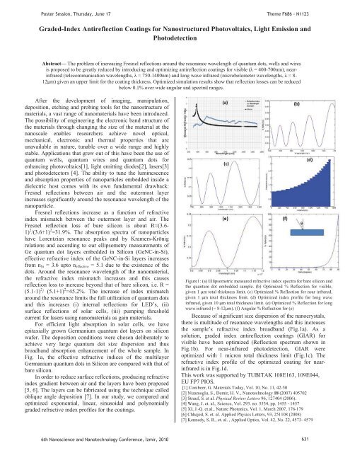
Poster Session, Thursday, June 17Theme F686 - N1123Graded-Index Antireflection Coat<strong>in</strong>gs for Nanostructured Photovoltaics, Light Emission andPhotodetectionAbstract— The problem of <strong>in</strong>creas<strong>in</strong>g Fresnel reflections around the resonance wavelength of quantum dots, wells and wiresis proposed to be greatly reduced by <strong>in</strong>troduc<strong>in</strong>g and optimiz<strong>in</strong>g antireflection coat<strong>in</strong>gs for visible ( = 400-700nm), near<strong>in</strong>frared(telecommunication wavelengths, = 750-1400nm) and long wave <strong>in</strong>frared (microbolometer wavelengths, = 8-12m) given an upper limit for the coat<strong>in</strong>g thickness. Optimized simulation results show that reflection losses can be reducedbelow 0.1% over wide angular and spectral ranges.After the development of imag<strong>in</strong>g, manipulation,deposition, etch<strong>in</strong>g and prob<strong>in</strong>g tools for the nanostructure ofmaterials, a vast range of nanomaterials have been <strong>in</strong>troduced.The possibility of eng<strong>in</strong>eer<strong>in</strong>g the electronic band structure ofthe materials through chang<strong>in</strong>g the size of the material at thenanoscale enables researchers achieve novel optical,mechanical, electronic and thermal properties that areunavailable <strong>in</strong> nature, tunable over a wide range and highlystable. Applications that grew out of this have been the use ofquantum wells, quantum wires and quantum dots forenhanc<strong>in</strong>g photovoltaics[1], light emitt<strong>in</strong>g diodes[2], lasers[3]and photodetectors [4]. The ability to tune the lum<strong>in</strong>escenceand absorption properties of nanoparticles embedded <strong>in</strong>side adielectric host comes with its own fundamental drawback:Fresnel reflections between air and the outermost layer<strong>in</strong>creases significantly around the resonance wavelength of thenanoparticle.Fresnel reflections <strong>in</strong>crease as a function of refractive<strong>in</strong>dex mismatch between the outermost layer and air. TheFresnel reflection loss of bare silicon is about R=(3.6-1) 2 /(3.6+1) 2 =31.9%. The absorption spectra of nanoparticleshave Lorentzian resonance peaks and by Kramers-Krönigrelations and accord<strong>in</strong>g to our ellipsometry measurements ofGe quantum dot layers embedded <strong>in</strong> Silicon (GeNC-<strong>in</strong>-Si),effective refractive <strong>in</strong>dex of the GeNC-<strong>in</strong>-Si layers <strong>in</strong>creasesfrom n Si = 3.6 upto n effective = 5.1 due to the existence of thedots. Around the resonance wavelength of the nanomaterial,the refractive <strong>in</strong>dex mismatch <strong>in</strong>creases and this causesreflection loss to <strong>in</strong>crease beyond that of bare silicon, i.e. R =(5.1-1) 2 / (5.1+1) 2 =45.2%. The <strong>in</strong>crease of <strong>in</strong>dex mismatcharound the resonance limits the full utilization of quantum dotsand this <strong>in</strong>creases (i) <strong>in</strong>ternal reflections for LED’s, (ii)surface reflections of solar cells, (iii) pump<strong>in</strong>g thresholdcurrent for lasers us<strong>in</strong>g nanomaterials as ga<strong>in</strong> materials.For efficient light absorption <strong>in</strong> solar cells, we haveepitaxially grown Germanium quantum dot layers on siliconwafer. The deposition conditions were chosen deliberately toachieve very large quantum dot size dispersion and thusbroadband absorption enhancement of the whole sample. InFig. 1a, the effective refractive <strong>in</strong>dices of the multilayerGermanium quantum dots <strong>in</strong> Silicon are compared with that ofbare silicon.In order to reduce surface reflections, produc<strong>in</strong>g refractive<strong>in</strong>dex gradient between air and the layers have been proposed[5, 6]. The layers can be fabricated us<strong>in</strong>g the technique calledoblique angle deposition [7]. In our study, we compared andoptimized exponential, l<strong>in</strong>ear, s<strong>in</strong>usoidal and polynomiallygraded refractive <strong>in</strong>dex profiles for the coat<strong>in</strong>gs.Figure1: (a) Ellipsometric measured refractive <strong>in</strong>dex spectra for bare silicon andthe quantum dot embedded sample. (b) Optimized % Reflection for visible,given 1 m total thickness limit. (c) Optimized % Reflection for near <strong>in</strong>frared,given 1 m total thickness limit. (d) Optimized <strong>in</strong>dex profile for long wave<strong>in</strong>frared, given 10 m total thickness limit. (e) Optimized % Reflection for longwave <strong>in</strong>frared (= 8-12m). (f) Angular % Reflection for (e)Because of significant size dispersion of the nano<strong>crystals</strong>,there is multitude of resonance wavelengths and this <strong>in</strong>creasesthe sample’s refractive <strong>in</strong>dex broadband (Fig.1a). As asolution, graded <strong>in</strong>dex antireflection coat<strong>in</strong>gs (GIAR) forvisible have been optimized (Reflection spectrum shown <strong>in</strong>Fig.1b). For near-<strong>in</strong>frared photodetection, GIAR wereoptimized with 1 micron total thickness limit (Fig.1c). Therefractive <strong>in</strong>dex profile of the optimized coat<strong>in</strong>g for near<strong>in</strong>fraredis <strong>in</strong> Fig.1d.This work was supported by TUBITAK 108E163, 109E044,EU FP7 PIOS.[1] Conibeer, G. Materials Today, Vol. 10, No. 11, 4250[2] Nizamoglu, S., Demir, H. V., Nanotechnology 18 (2007) 405702[3] Strauf, S. et al. Physical Review Letters 96, 127404 (2006).[4] Wang, J. et. al., Science, Vol. 293. no. 5534, pp. 1455 - 1457[5] XI, J.Q. et.al., Nature <strong>Photonic</strong>s, Vol. 1, March 2007, 176179[6] Chhajed, S. et. al. Applied Physics Letters, 93, 251108 (2008)[7] Kennedy, S. R., et. al. , Applied Optics, Vol. 42, No. 22, 4573 45796th Nanoscience and Nanotechnology Conference, zmir, 2010 631


