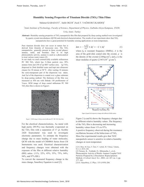
Poster Session, Thursday, June 17Theme F686 - N1123Humidity Sens<strong>in</strong>g Properties of Titanium Dioxide (TiO 2 ) Th<strong>in</strong> FilmsMehmet KABADAYI 1 , Salih OKUR 1 ,Nesli T. YAĞMURCUKARDEŞ 11 Izmir Institute of Technology, Faculty of Science, Department of Physics, Gulbahce Koyu Kampusu, 35430,Urla, Izmir, TurkeyAbstract- Humidity sens<strong>in</strong>g properties of TiO 2 nanoparticle th<strong>in</strong> film that prepared by drop cast<strong>in</strong>g method were <strong>in</strong>vestigatedby quartz crystal microbalance (QCM) and electrical characterization. The results of our experiment show that TiO 2nanoparticles have a great potential for humidity sens<strong>in</strong>g applications at room temperature.Pure titanium dioxide does not occur <strong>in</strong> nature but isderived from ilmenite of leuxocene ores. The TiO 2nanoparticles generally present <strong>in</strong> three crystal phases:anatase, rutile, and brookite. Due to its highphotocatalytic activity, anatase is used as a photocatalystto treat various waste waters [2].In our study we used commercially available millenniumPC 500 TiO 2 which has 5-10nm particle size, 99%anatase form and 250 m 2 /gr BET surface area. 1gr TiO 2dispersed <strong>in</strong> 20ml distilled water and kept <strong>in</strong>to ultrasoniccleaner for 30 m<strong>in</strong>ute at 50 0 C. After wait<strong>in</strong>g 10 m<strong>in</strong>utesthe semi-transparant part of the dispersion was taken.And 5μl of the dispersion is coated over a glass substrateby drop-cast<strong>in</strong>g method. The thickness of the film wasmeasured as 450 nm with Dektak 150 profilometer ofVeeco. SEM image of drop casted millenium PC 500TiO 2 th<strong>in</strong> film is shown <strong>in</strong> Figure1.(1)where is resonant frequency (8MHz), A is thearea of the gold disk coated onto the crystal, ρ isthe density of the crystal (2.684g/cm 3 ), and μ is theshear modulus of quartz (2.947x10 11 g/cms 2 ).F/Hz20-2-4-611%22%43%53%84%75%94%84%94%97%-80 1000 2000 3000 4000 5000 6000210(a)Time/sec43%53%75%22%11%y = 0,698 - 0,067407x R= 0,9972y = 2,2276 - 0,077601x R= 0,99245(b)-1f/Hz-2-3-4-5upwarddownward-60 20 40 60 80 100Relative Humidity (%)Figure 2(aand b):Frequency change with different RH(%) valuesFigure 1. SEM image of drop casted millenium PC 500 TiO2 th<strong>in</strong> film.For the electrical characterizations, Au metal withhigh purity (99.9%) was thermally evaporated onthe TiO 2 film with a separation of 17 μl. Keithly2420 Sourcemeter was used to <strong>in</strong>vestigateelectronic parameters. To estimate the frequencychange due to mass load<strong>in</strong>g of water molecules,QCM with the model of CHI400A Series from CHInstruments was used. Electrical characterizationand frequency changes were obta<strong>in</strong>ed with theexposure of the film at different relative humidity(RH) ratios. (11%, 22%, 43%, 55%, 75%, 84%,94%, and 97% RH.)To convert the measured frequency change to themass change, Sauerbrey Equation is used [3].Figure 2 (a and b) shows the frequency changes dueto different relative humidity values .The frequencyof the TiO 2 film is decreas<strong>in</strong>g and <strong>in</strong>creas<strong>in</strong>ghumidity values from 11% to 97%.A positive frequency observed dur<strong>in</strong>g the resonanceoscillations because of the behaviours of TiO 2films.Our experimental results give that TiO2nanoparticle sensor is sensitive to relative humiditychanges at room temperature[1] S. Okur, M. Kus, F. Özel, V. Aybek, M. Yilmaz, Talanta,81;1-2; 2010; 248.[2] Tetsuro, K., Toshiaki, O., Mitsunobu, I., et al.,Photocatalytic Activity of Rutile–Anatase Coupled TiO2Particles Prepared by a Dissolution–ReprecipitationMethod, J.Colloid. Interf. Sci., 2003, vol. 267, no. 2, pp.377–381.[3] G. Sauerbrey, Z. Phys. 155 (1959) 206.6th Nanoscience and Nanotechnology Conference, zmir, 2010 701
PPPPPPoster Session, Thursday, June 17Theme F686 - N1123Electrical and Optical Properties of Al Doped ZnO Film and Potential Applications of Gas Sensors1,21,21,21,2UO. SancakogluUPP*, M. ErolPP, M. BektasPP, F. EbeoglugilPP, H. SozbilenP3P, O. Mermer 2,3P, E. Celik 1,21PDokuz Eylul University, Department of Metallurgical and Materials Eng<strong>in</strong>eer<strong>in</strong>g, T<strong>in</strong>aztepe Campus, 35160 Buca, Izmir-Turkey.2PDokuz Eylul University, Center for Fabrication and Application of Electronic Materials (EMUM), T<strong>in</strong>aztepe Campus, 35160Buca, Izmir-Turkey3PEge University, Deparment of Electrical and Electronics Eng<strong>in</strong>eer<strong>in</strong>g, 35100, Bornova, Izmir-Turkey.Abstract-Undoped and Al doped semiconductor ZnO films on Si(100) and glass substrates were prepared by sol-gel technique. For thispropose, transparent solutions were prepared with Zn and Al based precursors. The solutions were deposited on glass substrates us<strong>in</strong>g sp<strong>in</strong>coat<strong>in</strong>g technique which decreases the film thickness up to nanoscale and gives the coat<strong>in</strong>g a smooth characteristic. Deposited films were driedooat 300P PC for 10 m<strong>in</strong> <strong>in</strong> order to remove hydrous and volatile content, subsequently films were heat treated at 500P PC for 5 m<strong>in</strong>. to removeoorganic contents and then to obta<strong>in</strong> ZnO phase structure the films were annealed at 600P PC for 1 hour <strong>in</strong> air atmosphere. F<strong>in</strong>ally the surfacemorphologies and roughness values of the films were determ<strong>in</strong>ed via AFM (atomic force microscopy) and profilometer, respectively. Thestructural and optical properties of these films have been <strong>in</strong>vestigated by XRD (x-ray diffractometer) and optical properties such astransmittance spectrum, optical band gap, and optical constants (refractive <strong>in</strong>dex, ext<strong>in</strong>ction coefficient, real and imag<strong>in</strong>ary parts of the dielectricconstant) of the films were determ<strong>in</strong>ed.Z<strong>in</strong>c oxide (ZnO) has attracted extensive <strong>in</strong>terest becauseof its important role <strong>in</strong> various applications, for example, gassensor [1], varistors [2], surface acoustic wave devices [3],optical waveguides [4] as well as blue/UV light emitt<strong>in</strong>gdevices [5]. In addition, ZnO has been considered as anexcellent candidate to replace <strong>in</strong>dium t<strong>in</strong> oxide (ITO) and t<strong>in</strong>oxide (SnO2) as transparent conductive electrodes <strong>in</strong> flat paneldisplay and solar cell devices [6,7]. The advantages of z<strong>in</strong>coxide <strong>in</strong>clude <strong>in</strong>expensiveness and relative ease oflithography. However, the electrical conductivity of un-dopedz<strong>in</strong>c oxide is not high enough for practical application. Furtherreduction of resistivity of z<strong>in</strong>c oxide can be achieved either bydop<strong>in</strong>g group III elements such as B, Al, In and Ga to replacez<strong>in</strong>c atoms [8] or group IV elements, F, to substitute oxygenatoms [9].The structural and morphological properties ofsemiconductor oxides have a substantial effect on their optical,electrical and gas sens<strong>in</strong>g properties. The controlledparticlesize and morphology facilitate the desired characteristics <strong>in</strong>the materials. Several simplewet chemical routes like sol–gel,co-precipitation and Pech<strong>in</strong>i route have been adapted to formnanostructures [10].specific acid-alcohol medium to remove the contam<strong>in</strong>ationsand prepare the surface for sol-gel coat<strong>in</strong>g. The films weredeposited by the technique detailed <strong>in</strong> Figure 1.Figure 2 shows the x-ray diffraction spectra of the pureZnO film. It also represents the success of the coat<strong>in</strong>g process.Figure 2. X-ray diffraction spectra of the pure ZnO film.The structural and optical properties of the films will beshown <strong>in</strong> details. b)The authors are <strong>in</strong>debted to State Plann<strong>in</strong>g Foundation(DPT) and Dokuz Eylul University for f<strong>in</strong>ancial support.*Correspond<strong>in</strong>g author: orkut.sancakoglu@deu.edu.trFigure 1. Flow chart of sol-gel process<strong>in</strong>g for ZnO th<strong>in</strong> films.In the present study; pure, and Al substituted ZnOR Rth<strong>in</strong> filmswere deposited on glass substrates by sol-gel method and sp<strong>in</strong>coat<strong>in</strong>g technique. Si(100) and glass substrates weremechanically cleaned by us<strong>in</strong>g a new designed apparatus <strong>in</strong> a[1] K.S. Weibenrieder, J. Muller, Th<strong>in</strong> Solid Films 30 (1997) 30.[2] E. Olsson, L.K.L. Falk, G.L. Dunlop, R. Osterlund, J. Mater. Sci.20 (1985) 4091.[3] C.R. Gorla, N.W. Emanetoglu, S. Liang, W.E. Mayo, Y. Lu, M.Wraback, H. Shen, J. Appl. Phys. 85 (1999) 2595.[4] M.H. Koch, P.Y. Timbrell, R.N. Lamb, Semicond. Sci. Technol.10 (1995) 1523.[5] D.C. Look, D.C. Reynolds, C.W. Litton, R.L. Jones, D.B. Easton,G. Cantwell, Appl. Phys. Lett. 81 (2002) 1830.[6] G. Hass, J. Heaney, A.R. Toft, Appl. Opt. 18 (1975) 1488.[7] R. Barber, G. Pryor, E. Re<strong>in</strong>heimer, SID Digest Tech. 28 (1997)18.[8] G. Sberveglieri, B. Benussi, G. Coccoli, S. Groppelli, P. Nelli,Th<strong>in</strong> Solid Films 186 (1990) 349.[9] C. Grivas, S. Mailis, L. Boutsikaris, D.S. Gill, N.A. Va<strong>in</strong>os, P.J.Chandler, Laser Phys. 8 (1998) 326.[10] C. S. Navale, V. Ravi, I.S. Mulla, Sensors and Actuators B 139(2009) 466–4706th Nanoscience and Nanotechnology Conference, zmir, 2010 702
- Page 1:
Poster Presentations3rd Day17 June
- Page 4 and 5:
Determination of Dielectric Anisotr
- Page 7 and 8:
Poster Session, Thursday, June 17Th
- Page 9 and 10:
PP mPP vs.P =P,PP (1)P andPoster Se
- Page 11 and 12:
PP mPP vs.P =P,PP (1)P andPoster Se
- Page 13 and 14:
PP andPoster Session, Thursday, Jun
- Page 15 and 16:
Poster Session, Thursday, June 17Th
- Page 17 and 18:
PP and770 772 774 776 778 780 782 7
- Page 19 and 20:
Poster Session, Thursday, June 17Th
- Page 21 and 22:
Poster Session, Thursday, June 17Th
- Page 23 and 24:
P25,Poster Session, Thursday, June
- Page 25 and 26:
PP TOBBPoster Session, Thursday, Ju
- Page 27 and 28:
PisPPisisisP,PisPoster Session, Thu
- Page 29 and 30:
U NeslihanPPPPoster Session, Thursd
- Page 31 and 32:
Poster Session, Thursday, June 17Th
- Page 33 and 34:
PPPoster Session, Thursday, June 17
- Page 35 and 36:
PPoster Session, Thursday, June 17T
- Page 37 and 38:
P onP viaPP wereP upPoster Session,
- Page 39 and 40:
P ·cm.PVPPPsPPPPP andPoster Sessio
- Page 41 and 42: Poster Session, Thursday, June 17Th
- Page 43 and 44: PPoster Session, Thursday, June 17T
- Page 45 and 46: PPoster Session, Thursday, June 17T
- Page 47 and 48: Poster Session, Thursday, June 17Th
- Page 49 and 50: PErkanPoster Session, Thursday, Jun
- Page 51 and 52: Poster Session, Thursday, June 17Th
- Page 53 and 54: Poster Session, Thursday, June 17Th
- Page 55 and 56: PPPP andPoster Session, Thursday, J
- Page 57 and 58: Poster Session, Thursday, June 17Th
- Page 59 and 60: Poster Session, Thursday, June 17Th
- Page 61 and 62: T PeptideTPP,PP,PP andTT2429TTTTTT
- Page 63 and 64: Poster Session, Thursday, June 17Th
- Page 65 and 66: PPoster Session, Thursday, June 17T
- Page 67 and 68: Poster Session, Thursday, June 17Th
- Page 69 and 70: PPPoster Session, Thursday, June 17
- Page 71 and 72: Poster Session, Thursday, June 17Th
- Page 73 and 74: Poster Session, Thursday, June 17Th
- Page 75 and 76: PT AdditionalT ThePoster Session, T
- Page 77 and 78: Poster Session, Thursday, June 17Th
- Page 79 and 80: Poster Session, Thursday, June 17Th
- Page 81 and 82: Poster Session, Thursday, June 17Th
- Page 83 and 84: PPoster Session, Thursday, June 17T
- Page 85 and 86: Poster Session, Thursday, June 17Th
- Page 87 and 88: PPPoster Session, Thursday, June 17
- Page 89 and 90: Poster Session, Thursday, June 17Hu
- Page 91: Poster Session, Thursday, June 17Th
- Page 95 and 96: Poster Session, Thursday, June 17Th
- Page 97 and 98: Poster Session, Thursday, June 17Th
- Page 99 and 100: Poster Session, Thursday, June 17Th
- Page 101 and 102: PPoster Session, Thursday, June 17T
- Page 103 and 104: Poster Session, Thursday, June 17Th
- Page 105 and 106: PPPPPPPoster Session, Thursday, Jun
- Page 107 and 108: Poster Session, Thursday, June 17Th
- Page 109 and 110: PPPR2R PIN(80)PPgPP OzlemPPoster Se
- Page 111 and 112: Poster Session, Thursday, June 17Th
- Page 113 and 114: Poster Session, Thursday, June 17Th
- Page 115 and 116: P onPP toP coordinatedPPoster Sessi
- Page 117 and 118: PPPPP,PP,P(PR RmPoster Session, Thu
- Page 119 and 120: Poster Session, Thursday, June 17Th
- Page 121 and 122: Poster Session, Thursday, June 17Th
- Page 123 and 124: PP InstitutePP DepartmentPoster Ses
- Page 125 and 126: andPCPPoster Session, Thursday, Jun
- Page 127 and 128: PP scatteringPYusufPP Corresponding
- Page 129 and 130: PP toPoster Session, Thursday, June
- Page 131 and 132: PP andPoster Session, Thursday, Jun
- Page 133 and 134: PPPPoster Session, Thursday, June 1
- Page 135 and 136: PPoster Session, Thursday, June 17T
- Page 137 and 138: PPP andP (.cm).Poster Session, Thur
- Page 139 and 140: PP tiltP andP editionPoster Session
- Page 141 and 142: PP andPPoster Session, Thursday, Ju
- Page 143 and 144:
Poster Session, Thursday, June 17Th
- Page 145 and 146:
PP forP forP edit.PPoster Session,
- Page 147 and 148:
Poster Session, Thursday, June 17Th
- Page 149 and 150:
Poster Session, Thursday, June 17Th
- Page 151 and 152:
PP ionicPP ,PPoster Session, Thursd
- Page 153 and 154:
PP lightPoster Session, Thursday, J
- Page 155 and 156:
Poster Session, Thursday, June 17Th
- Page 157 and 158:
PPoster Session, Thursday, June 17T
- Page 159 and 160:
Poster Session, Thursday, June 17Th
- Page 161 and 162:
PandPoster Session, Thursday, June
- Page 163 and 164:
Poster Session, Thursday, June 17 T
- Page 165 and 166:
PPPoster Session, Thursday, June 17
- Page 167 and 168:
PPoster Session, Thursday, June 17T
- Page 169 and 170:
PPoster Session, Thursday, June 17T
- Page 171 and 172:
PPoster Session, Thursday, June 17T
- Page 173 and 174:
PP DepartmentNanoscienceTPPoster Se
- Page 175 and 176:
Poster Session, Thursday, June 17Th
- Page 177 and 178:
Poster Session, Thursday, June 17Th
- Page 179 and 180:
PPPoster Session, Thursday, June 17
- Page 181 and 182:
PPPPPoster Session, Thursday, June
- Page 183 and 184:
PPPPoster Session, Thursday, June 1
- Page 185 and 186:
PPoster Session, Thursday, June 17T
- Page 187 and 188:
PPoster Session, Thursday, June 17T
- Page 189 and 190:
PPoster Session, Thursday, June 17T
- Page 191 and 192:
Poster Session, Thursday, June 17Th
- Page 193 and 194:
Poster Session, Thursday, June 17Th
- Page 195 and 196:
0T0T0T0T AsPPPP werePoster Session,
- Page 197 and 198:
PPoster Session, Thursday, June 17T
- Page 199 and 200:
PPPPPoster Session, Thursday, June
- Page 201 and 202:
PPoster Session, Thursday, June 17T
- Page 203 and 204:
PPoster Session, Thursday, June 17T
- Page 205 and 206:
Poster Session, Thursday, June 17Th
- Page 207 and 208:
PPoster Session, Thursday, June 17T
- Page 209 and 210:
PPoster Session, Thursday, June 17T
- Page 211:
Poster Session, Thursday, June 17AF