

Photonic crystals in biology - NanoTR-VI
Photonic crystals in biology - NanoTR-VI
Photonic crystals in biology - NanoTR-VI
- No tags were found...

You also want an ePaper? Increase the reach of your titles
YUMPU automatically turns print PDFs into web optimized ePapers that Google loves.
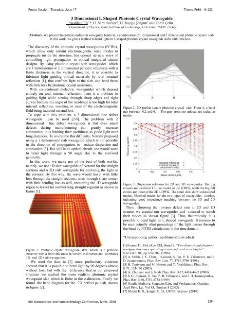
U NeslihanPPPPoster Session, Thursday, June 17Theme F686 - N112313 Dimensional L Shaped <strong>Photonic</strong> Crystal Waveguide111EtiUP P*, H. Sami SözüerP PP and Zebih Çet<strong>in</strong>PPAbstract- We present theoretical studies on waveguide bends <strong>in</strong> a comb<strong>in</strong>ation of 1 dimensional and 2 dimensional photonic crystal slab.In this work, we give a method to bend light on L shaped photonic crystal waveguide slabs with little loss.1The discovery of the photonic crystal waveguides (PCWs),which allow only certa<strong>in</strong> electromagnetic wave modes topropagate <strong>in</strong>side the structure, has opened up new ways ofcontroll<strong>in</strong>g light propagation <strong>in</strong> optical <strong>in</strong>tegrated circuitdesigns. By us<strong>in</strong>g photonic crystal slab waveguides, whichare 1 dimensional or 2 dimensional periodic structures with af<strong>in</strong>ite thickness <strong>in</strong> the vertical direction, it is possible tofabricate light guid<strong>in</strong>g optical materials by total <strong>in</strong>ternalreflection [1], that conf<strong>in</strong>es light to the slab, and bend themwith little loss by photonic crystal assistance.With conventional dielectric waveguides which dependentirely on total <strong>in</strong>ternal reflection, there is a problem <strong>in</strong>guid<strong>in</strong>g light while turn<strong>in</strong>g through sharp edges and tightcurves because the angle of the <strong>in</strong>cidence is too high for total<strong>in</strong>ternal reflection, result<strong>in</strong>g <strong>in</strong> most of the electromagneticfield be<strong>in</strong>g radiated out and lost.To cope with this problem, a 2 dimensional l<strong>in</strong>e defectwaveguide can be used [2-8]. The problem with 2dimensional l<strong>in</strong>e defect waveguides is that even smalldefects dur<strong>in</strong>g manufactur<strong>in</strong>g can greatly <strong>in</strong>creaseattenuation, thus limit<strong>in</strong>g their usefulness to guide light overlong distances. To overcome this difficulty, Notomi proposedus<strong>in</strong>g a 1 dimensional slab waveguide which is not periodic<strong>in</strong> the direction of propagation, to reduce dispersion andattenuation [3]. But still <strong>in</strong> an optical circuit, one would wantto bend light through a 90 angle due to the conf<strong>in</strong>edgeometry.In this work, we make use of the best of both worlds,namely, we use 1D slab waveguide of Notomi for the straightsections and a 2D slab waveguide for conta<strong>in</strong>ig the light atthe corners. By this way, the wave would travel with littleloss through the straight sections, turns through sharp cornerwith little bend<strong>in</strong>g loss as well, reenter<strong>in</strong>g the 1D waveguideregion to travel for another long straight segment as shown <strong>in</strong>figure [1].Figure 2. 2D perfect square photonic crystal slab. There is a bandgap between 0.2 and 0.4 . The gray areas are unlocalized radiationmodes.Figure 3. Dispersion relations for 2D and 1D waveguides. The bigcrosses are localized TE-like modes of the 1DWG, while the big fullcircles are those of the 2D LDWG. The small dots show unlocalizedmodes. Matched modes for the two types of waveguides overlap,<strong>in</strong>dicat<strong>in</strong>g good impedance match<strong>in</strong>g between the 1D and 2Dwaveguides.Then choos<strong>in</strong>g the proper defect size at 2D and 1Dstructes we created our waveguides and succeed to matchtheir modes as shown figure [3]. Thus, theoretically it ispossible to bend light <strong>in</strong> L shaped waveguide. It rema<strong>in</strong>s tobe seen actually what percentage of the light passes throughthe bend by FDTD calculations <strong>in</strong> the time doma<strong>in</strong>.*Correspond<strong>in</strong>g author: 2Tneslihaneti@iyte.edu.tr2TFigure 1. <strong>Photonic</strong> crystal waveguide slab, which is a periodicstructure with a f<strong>in</strong>ite thickness <strong>in</strong> vertical z-direction and comb<strong>in</strong>es1D and 2D slab waveguides.We used the data <strong>in</strong> [7] s<strong>in</strong>ce prelim<strong>in</strong>ary evidenceshowed that it is possible to bend light by 90 degrees almostwithout loss, but with the difference that <strong>in</strong> our proposedstructure we studied the more realistic photonic crystalwaveguide slab which is f<strong>in</strong>ite <strong>in</strong> the z-direction. Firstly wefound the band diagram for the 2D perfect pc slab, shown<strong>in</strong> figure [2].[1]2TKrauss TF, DeLaRue RM, Brand S, "Two-dimensional photonicbandgapstructures operat<strong>in</strong>g at near <strong>in</strong>frared wavelengths"NATURE 383 pp. 699-702, (1996)[2] A. Mekis, J. C. Chen, I. Kurland, S. Fan, P. R. Villeneuve, and J.D. Joannopoulos, Phys. Rev. Lett. 77, 3787-3790 (1996).[3] H. Taniyama and M. Natomi and Y. Yoshhikuni, Phys. Rev.B.71, 153-103 (2005).[4] A. Chut<strong>in</strong>an and S. Noda Phys. Rev.B.62, 4488-4492 (2000).[5] S. G. Jhonson, S. Fan, P. R. Villeneuve, and J. D. Joannopoulos,Phys. Rev.B.60, 5751-5758 (1999)[6] Natalia Malkova, Sungwon Kim, and Venkatraman Gopalan,Appl Phys. Let. Vol 83, Number 8 (2003)6th Nanoscience and Nanotechnology Conference, zmir, 2010 639


