PPPPPP*PP,PP andPoster Session, Thursday, June 17Theme F686 - N1123Topological Analysis of the Integer Quantum Hall Effect12,341UAyl<strong>in</strong> YildizUPP, Afif SiddikiPPDeniz EksiP Ismail SokmenP1 Department of Physics, Dokuz Eylul University, Izmir 35160, Turkey2PDepartment of Physics, Istanbul University, Istanbul 34134, TurkeyPDepartment of Physics, Harvard University, Cambridge MA 02138, USA4PDepartment of Physics, Trakya University, Edirne 22030, Turkey3Abstract-We discuss the role of topology on the <strong>in</strong>teger quantum Hall effect (IQHE). The characteristics of the edges as well as the bulkstates <strong>in</strong> a Hall bar with two identical square gates <strong>in</strong> the <strong>in</strong>terior and a Corb<strong>in</strong>o disc geometries with and without disorder have been analyzed<strong>in</strong> detail. The current distribution obta<strong>in</strong>ed from the L<strong>in</strong>ear Response Theory (LRT) is presented for all systems.Vortices <strong>in</strong> Type II superconductors, Aharonov-Bohmeffect and many other examples put forward the important roleof topology <strong>in</strong> condensed matter physics. S<strong>in</strong>ce the discoveryof the quantum Hall effect [1], important topological<strong>in</strong>vestigations have been performed [2-5].The famous gauge <strong>in</strong>variance argument of Laughl<strong>in</strong> [2] isfundamental to the phenomena. Laughl<strong>in</strong>'s argument, focussedon a closed cyl<strong>in</strong>der with a strong magnetic field normal to itssurface, is threaded by a time dependent magnetic flux. Eachtime the flux was <strong>in</strong>creased by one flux quantum, an electronwas argued to be adiabatically transferred from the <strong>in</strong>side tothe outside edge of the cyl<strong>in</strong>der. This resulted <strong>in</strong> a flow ofelectrical current proportional to the electro-motive driv<strong>in</strong>gforce, with a precisely quantized coeffcient of proportionality -the Hall conductance [2]. The Laughl<strong>in</strong>'s argument waselaborated on by Halper<strong>in</strong> to a Corb<strong>in</strong>o disc - a hollow discshaped sample [3]. With<strong>in</strong> a Corb<strong>in</strong>o-disc geometry, thequantized Hall conductance could be understood as a discretetransfer of electrons between the <strong>in</strong>ner and outer edges, onefor each magnetic flux quantum thread<strong>in</strong>g the bore of the disc.The importance of the edge state was first demonstrated bythis work.The equivalence of Hall bar sample enclosed on itself underthe periodic boundary conditions as well as gauge <strong>in</strong>varianceand Corb<strong>in</strong>o disc topologies is one of the <strong>in</strong>trigu<strong>in</strong>g researchtopics. In this study we def<strong>in</strong>e two geometries - a Hall bar withidentical square gates <strong>in</strong> the <strong>in</strong>terior region and a Corb<strong>in</strong>o discas an annular 2DEG system surround<strong>in</strong>g a metallic contact[i.e., an electron reservoir (electrode)] and surrounded <strong>in</strong> turnby a second metallic contact as shown <strong>in</strong> Figure 1.The Hall bar geometry <strong>in</strong>volve a physical edge which connectsthe prob<strong>in</strong>g contacts. A unique feature of Corb<strong>in</strong>o disc is that,unlike other two-dimensional semiconductor devices, theirboundaries consist entirely of metallic contacts and no edgeconnects the contacts. This different sample configuration ledto the observation of completely different effects.The characteristics of the <strong>in</strong>compressible strips (IS) havebeen analyzed for both geometries with and without disorder.We apply the Thomas-Fermi Approximation (TFA) assum<strong>in</strong>gthe electrostatic quantities vary slowly <strong>in</strong> the quantummechanical scale such as magnetic length [7]. We obta<strong>in</strong>edcircular ISs <strong>in</strong> Corb<strong>in</strong>o disc near <strong>in</strong>ner and outer annulus atT=5K temperature under the <strong>in</strong>fluence of B=8T, whichobviously confirm the edge picture for Hall conductancestressed by Halper<strong>in</strong>. Under T=4K, B=8.5T conditions theobta<strong>in</strong>ed edge states <strong>in</strong> the clean Hall bar sample are parallelto the straight l<strong>in</strong>e connect<strong>in</strong>g source and dra<strong>in</strong>. On the otherhand, the circular edge states <strong>in</strong> Corb<strong>in</strong>o geometry cut thecorrespond<strong>in</strong>g l<strong>in</strong>e perpendicularly. With <strong>in</strong>creas<strong>in</strong>g magneticfield the existence of ISs <strong>in</strong> both systems is described by thebulk states. This picture is valid for a small magnetic fieldrange.In the presence of a small fixed current the system is locally<strong>in</strong> thermal equilibrium. In this case the l<strong>in</strong>earity between thecurrent density and the electric field is almost conserved thatthe L<strong>in</strong>ear Response theory (LRT) is valid [8]. The Hallcurrent <strong>in</strong> Hall bar sample is carried by edge states for B=7.5Tand T=6K conditions, while with <strong>in</strong>creas<strong>in</strong>g the magnetic fieldup to 8T current penetrates the ISs around the gates.Our calculations show that the existence of disorderbroadens the ISs and the bulk picture is ascendent <strong>in</strong> bothsystems <strong>in</strong>dependent of the geometry.In summary, we analyze the edge or bulk states realizationsof the IQHE <strong>in</strong> a Hall bar with two identical square gates <strong>in</strong>the <strong>in</strong>terior and a Corb<strong>in</strong>o disc geometries with and withoutdisorder. We conclude that the edge and bulk states areactually related and the topological characters of the Hall barand Corb<strong>in</strong>o disc systems are quite different.*Correspond<strong>in</strong>g author: HTayl<strong>in</strong>.yildiz@deu.edu.trTFigure 1. (a) Hall bar geometry with identical square gates <strong>in</strong> the<strong>in</strong>terior region (red squares). (b) Corb<strong>in</strong>o disc geometry. The blueregions <strong>in</strong>dicate the two-dimensional electron gas, the red areas aresource (S) and dra<strong>in</strong> (D) elements and the yellow squares denotes themetallic contacts <strong>in</strong> both samples.[1] K. Von Klitz<strong>in</strong>g, G. Dorda and M. Pepper, Phys. Rev. Lett. 45,494 (1980).[2] R. B. Laughl<strong>in</strong>, Phys. Rev. B 23(10), 5632 (1981).[3] B.I. Halper<strong>in</strong>, Phys. Rev. B 25, 2185 (1982).[4] G. Kirczenow, J.Phys.: Condens. Matter. 6, L583-L588 (1994).[5] E. Yahel, A. Plalevski, and H. Shtrikman, Superlattices andMicrostructures 22(4), 537 (1997).[7] A. Siddiki, R. R. Gerhardts, Phys. Rev. B 70 (2004) 195335.[8] K. Güven, R. R. Gerhardts, Phys. Rev. B 67 (2003) 115327.6th Nanoscience and Nanotechnology Conference, zmir, 2010 661
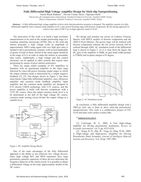
Poster Session, Thursday, June 17Theme F686 - N1123Fully Differential High Voltage Amplifier Design for Stick-slip Nanoposition<strong>in</strong>gNazmi Burak Budanur 1* , Devrim Yılmaz Aksın 1 , Oğuzhan Gürlü 21 Electronics & Communications Department, Istanbul Technical University, Istanbul 34469, Turkey2 Physics Department, Istanbul Technical University, Istanbul 34469, TurkeyAbstract – A fully differential high voltage amplifier to drive stick-slip piezoelectric actuators is designed. The amplifier consists of a fullydifferential amplifier and a common mode amplifier as ICs, and a power boost<strong>in</strong>g stage with discrete components. By this design approach weachieve slew rates of 300 V/μs on high capacitive loads of 10 nF.The motivation of this work is to build a high resolutionnanopositioner to be used <strong>in</strong> the sample position<strong>in</strong>g stage of ascann<strong>in</strong>g tunnel<strong>in</strong>g microscope (STM). Due to the stick-slipmotion pr<strong>in</strong>ciple, a high voltage (with an amplitude ofapproximately 300V) ramp signal with very high slew rates isneeded to drive piezoelectric ceramics with several hundredthsof grams of load on them. Period of the ramp signal should be<strong>in</strong> the range of 0.1s <strong>in</strong> order to make the motion <strong>in</strong> reasonabletime scales. Additionally, a high voltage and fast controlelectronic can be applied <strong>in</strong> other systems that require nanoposition<strong>in</strong>g by means of piezo electric positioners.There are s<strong>in</strong>gle ended examples of HV amplifiers <strong>in</strong>literature with an operational amplifier <strong>in</strong> the <strong>in</strong>put stagefollowed by class-AB power boost<strong>in</strong>g output stages <strong>in</strong> whichthe output common mode is determ<strong>in</strong>ed by a simple negativefeedback [1], [2]. Our design, shown <strong>in</strong> Figure 1, has threema<strong>in</strong> blocks: Input fully differential amplifier, class-AB poweramplifier and common mode feedback amplifier. Inputamplifier and the common mode amplifier are designed <strong>in</strong>0.35 micron CMOS technology with 3.3V sources, and thepower amplifier is build with discrete components with a155V DC source. S<strong>in</strong>ce the output common mode level is tobe determ<strong>in</strong>ed at the half of the high voltage DC source,common mode sens<strong>in</strong>g circuit divides the output voltage to asuitable level.We design and simulate our circuit on Cadence VirtuosoSpectre with SPICE models of discrete components and theAMS 0.35μm libraries. The power stage will be realized withdiscrete components whereas the low power sections will berealized through AMS. AC simulation result of the differentialloop is shown <strong>in</strong> Figure 2. As it is clear from the figure, theDC ga<strong>in</strong> of the amplifier is 90dB, its ga<strong>in</strong> band width productis 370kHz and its phase marg<strong>in</strong> is 83 degree.Figure 2. AC Simulation result.In conclusion, a fully differential amplifier design with a300V/μs slew rate is done to drive stick-slip piezoelectricnanopositioners. This work is a collaborative project of ITUVLSI and nano scale surface science labs.* budanur@itu.edu.tr[1] Colclough, M. S., 2000, A Fast high-voltageamplifier for driv<strong>in</strong>g piezoelectric positioners, Review ofScientific Instruments, vol.71 pp. 4323-4324[2] Wang, D. H., Zhu, W., Yang, Q., D<strong>in</strong>g, W.M., 2009,A High-voltage and High-power Amplifier for Driv<strong>in</strong>gPiezoelectric Stack Actuators, Journal of Intelligent MaterialSystems and Structures, Vol. 20 pp. 1987-2001Figure 1. HV Amplifier Design BlocksOne of the ma<strong>in</strong> advantages of the fully differentialapproach is the ability to use relatively low voltage devices.S<strong>in</strong>ce high voltage BJT and MOS transistors have largegeometries, parasitic capacitors of these devices determ<strong>in</strong>e thefrequency behavior of the whole circuit. It is possible to obta<strong>in</strong>a differential voltage on the load, approximately double of theDC source.6th Nanoscience and Nanotechnology Conference, zmir, 2010 662
- Page 1: Poster Presentations3rd Day17 June
- Page 4 and 5: Determination of Dielectric Anisotr
- Page 7 and 8: Poster Session, Thursday, June 17Th
- Page 9 and 10: PP mPP vs.P =P,PP (1)P andPoster Se
- Page 11 and 12: PP mPP vs.P =P,PP (1)P andPoster Se
- Page 13 and 14: PP andPoster Session, Thursday, Jun
- Page 15 and 16: Poster Session, Thursday, June 17Th
- Page 17 and 18: PP and770 772 774 776 778 780 782 7
- Page 19 and 20: Poster Session, Thursday, June 17Th
- Page 21 and 22: Poster Session, Thursday, June 17Th
- Page 23 and 24: P25,Poster Session, Thursday, June
- Page 25 and 26: PP TOBBPoster Session, Thursday, Ju
- Page 27 and 28: PisPPisisisP,PisPoster Session, Thu
- Page 29 and 30: U NeslihanPPPPoster Session, Thursd
- Page 31 and 32: Poster Session, Thursday, June 17Th
- Page 33 and 34: PPPoster Session, Thursday, June 17
- Page 35 and 36: PPoster Session, Thursday, June 17T
- Page 37 and 38: P onP viaPP wereP upPoster Session,
- Page 39 and 40: P ·cm.PVPPPsPPPPP andPoster Sessio
- Page 41 and 42: Poster Session, Thursday, June 17Th
- Page 43 and 44: PPoster Session, Thursday, June 17T
- Page 45 and 46: PPoster Session, Thursday, June 17T
- Page 47 and 48: Poster Session, Thursday, June 17Th
- Page 49 and 50: PErkanPoster Session, Thursday, Jun
- Page 51: Poster Session, Thursday, June 17Th
- Page 55 and 56: PPPP andPoster Session, Thursday, J
- Page 57 and 58: Poster Session, Thursday, June 17Th
- Page 59 and 60: Poster Session, Thursday, June 17Th
- Page 61 and 62: T PeptideTPP,PP,PP andTT2429TTTTTT
- Page 63 and 64: Poster Session, Thursday, June 17Th
- Page 65 and 66: PPoster Session, Thursday, June 17T
- Page 67 and 68: Poster Session, Thursday, June 17Th
- Page 69 and 70: PPPoster Session, Thursday, June 17
- Page 71 and 72: Poster Session, Thursday, June 17Th
- Page 73 and 74: Poster Session, Thursday, June 17Th
- Page 75 and 76: PT AdditionalT ThePoster Session, T
- Page 77 and 78: Poster Session, Thursday, June 17Th
- Page 79 and 80: Poster Session, Thursday, June 17Th
- Page 81 and 82: Poster Session, Thursday, June 17Th
- Page 83 and 84: PPoster Session, Thursday, June 17T
- Page 85 and 86: Poster Session, Thursday, June 17Th
- Page 87 and 88: PPPoster Session, Thursday, June 17
- Page 89 and 90: Poster Session, Thursday, June 17Hu
- Page 91 and 92: Poster Session, Thursday, June 17Th
- Page 93 and 94: PPPPPPoster Session, Thursday, June
- Page 95 and 96: Poster Session, Thursday, June 17Th
- Page 97 and 98: Poster Session, Thursday, June 17Th
- Page 99 and 100: Poster Session, Thursday, June 17Th
- Page 101 and 102: PPoster Session, Thursday, June 17T
- Page 103 and 104:
Poster Session, Thursday, June 17Th
- Page 105 and 106:
PPPPPPPoster Session, Thursday, Jun
- Page 107 and 108:
Poster Session, Thursday, June 17Th
- Page 109 and 110:
PPPR2R PIN(80)PPgPP OzlemPPoster Se
- Page 111 and 112:
Poster Session, Thursday, June 17Th
- Page 113 and 114:
Poster Session, Thursday, June 17Th
- Page 115 and 116:
P onPP toP coordinatedPPoster Sessi
- Page 117 and 118:
PPPPP,PP,P(PR RmPoster Session, Thu
- Page 119 and 120:
Poster Session, Thursday, June 17Th
- Page 121 and 122:
Poster Session, Thursday, June 17Th
- Page 123 and 124:
PP InstitutePP DepartmentPoster Ses
- Page 125 and 126:
andPCPPoster Session, Thursday, Jun
- Page 127 and 128:
PP scatteringPYusufPP Corresponding
- Page 129 and 130:
PP toPoster Session, Thursday, June
- Page 131 and 132:
PP andPoster Session, Thursday, Jun
- Page 133 and 134:
PPPPoster Session, Thursday, June 1
- Page 135 and 136:
PPoster Session, Thursday, June 17T
- Page 137 and 138:
PPP andP (.cm).Poster Session, Thur
- Page 139 and 140:
PP tiltP andP editionPoster Session
- Page 141 and 142:
PP andPPoster Session, Thursday, Ju
- Page 143 and 144:
Poster Session, Thursday, June 17Th
- Page 145 and 146:
PP forP forP edit.PPoster Session,
- Page 147 and 148:
Poster Session, Thursday, June 17Th
- Page 149 and 150:
Poster Session, Thursday, June 17Th
- Page 151 and 152:
PP ionicPP ,PPoster Session, Thursd
- Page 153 and 154:
PP lightPoster Session, Thursday, J
- Page 155 and 156:
Poster Session, Thursday, June 17Th
- Page 157 and 158:
PPoster Session, Thursday, June 17T
- Page 159 and 160:
Poster Session, Thursday, June 17Th
- Page 161 and 162:
PandPoster Session, Thursday, June
- Page 163 and 164:
Poster Session, Thursday, June 17 T
- Page 165 and 166:
PPPoster Session, Thursday, June 17
- Page 167 and 168:
PPoster Session, Thursday, June 17T
- Page 169 and 170:
PPoster Session, Thursday, June 17T
- Page 171 and 172:
PPoster Session, Thursday, June 17T
- Page 173 and 174:
PP DepartmentNanoscienceTPPoster Se
- Page 175 and 176:
Poster Session, Thursday, June 17Th
- Page 177 and 178:
Poster Session, Thursday, June 17Th
- Page 179 and 180:
PPPoster Session, Thursday, June 17
- Page 181 and 182:
PPPPPoster Session, Thursday, June
- Page 183 and 184:
PPPPoster Session, Thursday, June 1
- Page 185 and 186:
PPoster Session, Thursday, June 17T
- Page 187 and 188:
PPoster Session, Thursday, June 17T
- Page 189 and 190:
PPoster Session, Thursday, June 17T
- Page 191 and 192:
Poster Session, Thursday, June 17Th
- Page 193 and 194:
Poster Session, Thursday, June 17Th
- Page 195 and 196:
0T0T0T0T AsPPPP werePoster Session,
- Page 197 and 198:
PPoster Session, Thursday, June 17T
- Page 199 and 200:
PPPPPoster Session, Thursday, June
- Page 201 and 202:
PPoster Session, Thursday, June 17T
- Page 203 and 204:
PPoster Session, Thursday, June 17T
- Page 205 and 206:
Poster Session, Thursday, June 17Th
- Page 207 and 208:
PPoster Session, Thursday, June 17T
- Page 209 and 210:
PPoster Session, Thursday, June 17T
- Page 211:
Poster Session, Thursday, June 17AF