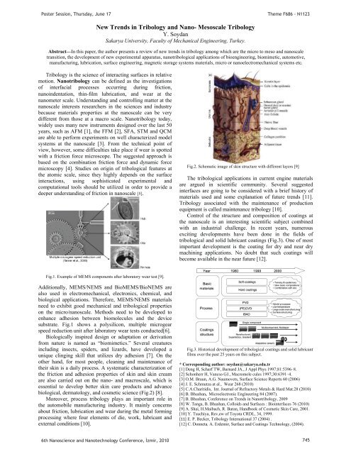
Poster Session, Thursday, June 17Theme F686 - N1123New Trends <strong>in</strong> Tribology and Nano- Mesoscale TribologyY. SoydanSakarya University, Faculty of Mechanical Eng<strong>in</strong>eer<strong>in</strong>g, Turkey.Abstract—In this paper, the author presents a review of new trends <strong>in</strong> tribology among which are the micro to meso and nanoscaletransition, the development of new experimental apparatus, nanotribological applications of bioeng<strong>in</strong>eer<strong>in</strong>g, biomimetic, automotive,manufactur<strong>in</strong>g, lubrication, surface eng<strong>in</strong>eer<strong>in</strong>g, magnetic storage systems materials, micro or nanoelectromechanical systems etc.Tribology is the science of <strong>in</strong>teract<strong>in</strong>g surfaces <strong>in</strong> relativemotion. Nanotribology can be def<strong>in</strong>ed as the <strong>in</strong>vestigationsof <strong>in</strong>terfacial processes occurr<strong>in</strong>g dur<strong>in</strong>g friction,nano<strong>in</strong>dentation, th<strong>in</strong>-film lubrication, and wear at thenanometer scale. Understand<strong>in</strong>g and controll<strong>in</strong>g matter at thenanoscale <strong>in</strong>terests researchers <strong>in</strong> the sciences and <strong>in</strong>dustrybecause materials properties at the nanoscale can be verydifferent from those at a macro scale. Nanotribology today,widely uses many new <strong>in</strong>struments designed over the last 50years, such as AFM [1], the FFM [2], SFA, STM and QCMare able to perform experiments on well characterized modelsystems at the nanoscale [3]. From the technical po<strong>in</strong>t ofview, however, some difficulties take place if wear is spottedwith a friction force microscope. The suggested approach isbased on the comb<strong>in</strong>ation friction force and dynamic forcemicroscopy [4]. Studies on orig<strong>in</strong> of tribological features atthe atomic scale, s<strong>in</strong>ce they highly depends on the surface<strong>in</strong>teractions, us<strong>in</strong>g sophisticated experimental andcomputational tools should be utilized <strong>in</strong> order to provide adeeper understand<strong>in</strong>g of friction <strong>in</strong> nanoscale [5].Fig.2. Schematic image of sk<strong>in</strong> structure with different layers [9]The tribological applications <strong>in</strong> current eng<strong>in</strong>e materialsare argued <strong>in</strong> scientific community. Several suggested<strong>in</strong>terfaces are go<strong>in</strong>g to be considered with a brief history ofmaterials used and some explanation of future trends [11].Tribology associated with the ma<strong>in</strong>tenance of productionequipment is called ma<strong>in</strong>tenance tribology [10].Control of the structure and composition of coat<strong>in</strong>gs atthe nanoscale is an <strong>in</strong>terest<strong>in</strong>g scientific subject comb<strong>in</strong>edwith an <strong>in</strong>dustrial challenge. In recent years, numerousexcit<strong>in</strong>g developments have been done <strong>in</strong> the fields oftribological and solid lubricant coat<strong>in</strong>gs (Fig.3). One of mostimportant development is the coat<strong>in</strong>g for dry and near drymach<strong>in</strong><strong>in</strong>g applications. No doubt that such coat<strong>in</strong>gs willbecome available <strong>in</strong> the near future [12].Fig.1. Example of MEMS components after laboratory wear test [9].Additionally, MEMS/NEMS and BioMEMS/BioNEMS arealso used <strong>in</strong> electromechanical, electronics, chemical, andbiological applications. Therefore, MEMS/NEMS materialsneed to exhibit good mechanical and tribological propertieson the micro/nanoscale. Methods need to be developed toenhance adhesion between biomolecules and the devicesubstrate. Fig.1 shows a polysilicon, multiple microgearspeed reduction unit after laboratory wear tests conducted[6].Biologically <strong>in</strong>spired design or adaptation or derivationfrom nature is named as “biomimetics.” Several creatures<strong>in</strong>clud<strong>in</strong>g <strong>in</strong>sects, spiders, and lizards, have developed aunique cl<strong>in</strong>g<strong>in</strong>g skill that utilizes dry adhesion [7]. On theother hand, for most people, clean<strong>in</strong>g and ma<strong>in</strong>tenance oftheir sk<strong>in</strong> is a daily process. A systematic characterization ofthe friction and adhesion properties of sk<strong>in</strong> and sk<strong>in</strong> creamare also carried out on the nano- and macroscale, which isessential to develop better sk<strong>in</strong> care products and advancebiological, dermatology, and cosmetic science (Fig.2) [8].Moreover, process tribology plays an important role <strong>in</strong>the automobile manufactur<strong>in</strong>g <strong>in</strong>dustry. It ma<strong>in</strong>ly concernsabout friction, lubrication and wear dur<strong>in</strong>g the metal form<strong>in</strong>gprocess<strong>in</strong>g where four elements of die, work, lubricant andexternal conditions [10].Fig.3. Historical development of tribological coat<strong>in</strong>gs and solid lubricantfilms over the past 25 years on this subject.* Correspond<strong>in</strong>g author: soydan@sakarya.edu.tr[1] Deng H, Scharf TW, Barnard JA., J Appl Phys 1997;81:5396–8.[2] Schonherr H, Vancso GJ., Macromole cules 1997;30:6391–4.[3] O.M. Braun, A.G. Naumovets, Surface Science Reports 60 (2006)[4] J. E. Schmutza at al., Wear 268 (2010)[5] C.A.Charitidis, Int. Journal of Refractory Metals & Hard Mat.28 (2010)[6] B. Bhushan, Microelectronic Eng<strong>in</strong>eer<strong>in</strong>g 84 (2007).[7] B. Bhushan, Conference on Trends <strong>in</strong> Nanotribology, 2009[8] W. Tanga, B. Bhushan, Colloids and Surfaces : Bio<strong>in</strong>terfaces 76 (2010)[9] A. Shai, H.Maibach, R. Baran, Handbook of Cosmetic Sk<strong>in</strong> Care, 2001.[10] Y. Tsuchiya, Rev,ew of Toyota CRDL, 34, 1999.[11] E. P. Becker, Tribology International 37 (2004) .[12] C. Donneta, A. Erdemir, Surface and Coat<strong>in</strong>gs Technology, (2004).6th Nanoscience and Nanotechnology Conference, zmir, 2010 745
PPP andP (.cm).Poster Session, Thursday, June 17Theme F686 - N11230BTemperature Dependent Electrical Conductivity of Ardel D-100 / MWCNT Nanocomposite121Murat ÇalkanP P, Dolunay akarPUMerih Ser<strong>in</strong>UP P*1PDepartment of Physics, Yildiz Technical University, stanbul 34210, Turkey2PDepartment of Chemistry, Yildiz Technical University, Istanbul 34210, TurkeyTAbstractT-In this work, ARDEL D-100/MWCNT (1.5 wt%) nanocomposite was studied. The characterization of the electrical properties ofprepared nanocomposite with respect to the temperature were studied. Direct-current measurements with a cont<strong>in</strong>uously chang<strong>in</strong>g temperatureof sample were presented. The resistivity of the ARDEL D-100 was decreased by 10 order of magnitude onaddition of 1.5wt%of MWCNT.Multiwalled carbon nanotubes (MWCNTs) areconsidered to be the ideal re<strong>in</strong>forc<strong>in</strong>g agent forhigh-strength polymer composites, because of theirfantastic mechanical strength, high electrical and thermalconductivity and high aspect ratio [1].ARDEL D-100 which is high eng<strong>in</strong>eer<strong>in</strong>g thermoplasticand an amorphous aromatic polyester of bisphenol-A withterephthalic and isophthalic acid (50/50) was studied. It hashigh heat-deflection temperature, high impact strength andgood electrical properties [2].Our aim was to obta<strong>in</strong> an <strong>in</strong>sight of the mechanism of theconductivity of ARDEL D-l00/MWCNT nanocompositeand to determ<strong>in</strong>e the characteristic glass transitiontemperature, Tg, of the sample. For this purpose, thecharacterization of the electrical properties of preparednanocomposite with respect to the temperature werestudied. Direct-current measurements with a cont<strong>in</strong>uouslychang<strong>in</strong>g temperature of sample were presented.ARDEL D-100/MWCNT (1.5 wt%) nanocomposite wasprepared by melt mix<strong>in</strong>g at 300 °C, 50 rpm <strong>in</strong> 5 m<strong>in</strong>. Thiswas carried out <strong>in</strong> the Leibniz Institute of Polymer ResearchDresden. The film of melt compounded ARDEL D – 100 /MWCNT (1.5wt%) nanocomposite was prepared viasolvent cast<strong>in</strong>g method on glass substrate.The volume resistivity of melt mix<strong>in</strong>g sample wasdeterm<strong>in</strong>ed by measur<strong>in</strong>g the DC resistance on the pressedplates. The measurement was performed on strips cut fromthe pressed sheets us<strong>in</strong>g a four-po<strong>in</strong>t text fixture comb<strong>in</strong>edwith a Keithley DMM 2000 electrometer. Prior to themeasurement, the surface of the sample was cleaned withethanol. This was carried out <strong>in</strong> The Leibniz Institute ofPolymer Research Dresden.For the electrical characterization, dark conductivity ofproduced films were measured as a function of temperatureus<strong>in</strong>g a Janis liquid nitrogen vacuum cryostat, hav<strong>in</strong>g athermocouple <strong>in</strong> good thermal contact with the sample.Samples were placed on top of a copper plate that is heatedby a bolt heater embedded with<strong>in</strong>.Temperature was controlled by Lakeshore TemperatureController 331. Dark conductivity measurements wereaccomplished us<strong>in</strong>g a programmable Keitley 6517A digitalelectrometer/voltage source <strong>in</strong>terfaced to a computer.The temperature dependence of conductivity wasmeasured as the temperature be<strong>in</strong>g <strong>in</strong>creased at a constant-1rate of 3K m<strong>in</strong>PP. The film thickness was determ<strong>in</strong>edfrom the area formed by spread<strong>in</strong>g polymer solution withknown volume and concentration.The change <strong>in</strong> the conductivity of the sample wasexperimentally measured under a constant electrical field.-6The measurements were carried out <strong>in</strong> l0PPTorr vacuum andthe dark. The electrical conductivity of the polymer wasmeasured <strong>in</strong> AI/ARDEL D-100/MWCNT/A1 structureover the temperature range of 300-520K.The volume resistivity of pure ARDEL D-100 was14measured as 1.54x10P The volume and specificresistivity of the nanocomposite sample was measured as453.5lxl0P P(.cm) and 8.56 xl0P P(.cm), respectively, at roomtemperature.In summary, we showed that the resistivity of the ARDELD-100 was decreased (conductivity <strong>in</strong>creased) by ten ordersof magnitude on addition of 1.5wt% MWCNT.The electrical conductivity values of ARDEL D-100/MWCNT with <strong>in</strong>creas<strong>in</strong>g temperature, which would beuseful for a wide range of applications, were achieved. Thisnanocomposite film showed semiconductor behavior withthe exponential variation of <strong>in</strong>verse temperaturedependence of electrical conductivity. Therefore, it ispossible to expla<strong>in</strong> the conduction mechanism of thenanocomposite by us<strong>in</strong>g exist<strong>in</strong>g solid state theory.This work was partially supported by the Leibniz Instituteof Polymer Research Dresden, and by Yildiz TechnicalUniversity, Scientific Research Project Coord<strong>in</strong>ation, underGrant No. BAPK-2001-01-01-01 andBAPK-2007-01-01-07.*Correspond<strong>in</strong>g author: ser<strong>in</strong>@vildiz.edu.tr[1] EW. Wong, PE. Sheehan, CM. Lieber. Science, 277:1971–5,(1997).[2] D. Sakar, O. Cankurtaran and F. Karaman, Journal ofApplied Polymer Science, 98(6): 2365-2368 (2005).6th Nanoscience and Nanotechnology Conference, zmir, 2010 746
- Page 1:
Poster Presentations3rd Day17 June
- Page 4 and 5:
Determination of Dielectric Anisotr
- Page 7 and 8:
Poster Session, Thursday, June 17Th
- Page 9 and 10:
PP mPP vs.P =P,PP (1)P andPoster Se
- Page 11 and 12:
PP mPP vs.P =P,PP (1)P andPoster Se
- Page 13 and 14:
PP andPoster Session, Thursday, Jun
- Page 15 and 16:
Poster Session, Thursday, June 17Th
- Page 17 and 18:
PP and770 772 774 776 778 780 782 7
- Page 19 and 20:
Poster Session, Thursday, June 17Th
- Page 21 and 22:
Poster Session, Thursday, June 17Th
- Page 23 and 24:
P25,Poster Session, Thursday, June
- Page 25 and 26:
PP TOBBPoster Session, Thursday, Ju
- Page 27 and 28:
PisPPisisisP,PisPoster Session, Thu
- Page 29 and 30:
U NeslihanPPPPoster Session, Thursd
- Page 31 and 32:
Poster Session, Thursday, June 17Th
- Page 33 and 34:
PPPoster Session, Thursday, June 17
- Page 35 and 36:
PPoster Session, Thursday, June 17T
- Page 37 and 38:
P onP viaPP wereP upPoster Session,
- Page 39 and 40:
P ·cm.PVPPPsPPPPP andPoster Sessio
- Page 41 and 42:
Poster Session, Thursday, June 17Th
- Page 43 and 44:
PPoster Session, Thursday, June 17T
- Page 45 and 46:
PPoster Session, Thursday, June 17T
- Page 47 and 48:
Poster Session, Thursday, June 17Th
- Page 49 and 50:
PErkanPoster Session, Thursday, Jun
- Page 51 and 52:
Poster Session, Thursday, June 17Th
- Page 53 and 54:
Poster Session, Thursday, June 17Th
- Page 55 and 56:
PPPP andPoster Session, Thursday, J
- Page 57 and 58:
Poster Session, Thursday, June 17Th
- Page 59 and 60:
Poster Session, Thursday, June 17Th
- Page 61 and 62:
T PeptideTPP,PP,PP andTT2429TTTTTT
- Page 63 and 64:
Poster Session, Thursday, June 17Th
- Page 65 and 66:
PPoster Session, Thursday, June 17T
- Page 67 and 68:
Poster Session, Thursday, June 17Th
- Page 69 and 70:
PPPoster Session, Thursday, June 17
- Page 71 and 72:
Poster Session, Thursday, June 17Th
- Page 73 and 74:
Poster Session, Thursday, June 17Th
- Page 75 and 76:
PT AdditionalT ThePoster Session, T
- Page 77 and 78:
Poster Session, Thursday, June 17Th
- Page 79 and 80:
Poster Session, Thursday, June 17Th
- Page 81 and 82:
Poster Session, Thursday, June 17Th
- Page 83 and 84:
PPoster Session, Thursday, June 17T
- Page 85 and 86: Poster Session, Thursday, June 17Th
- Page 87 and 88: PPPoster Session, Thursday, June 17
- Page 89 and 90: Poster Session, Thursday, June 17Hu
- Page 91 and 92: Poster Session, Thursday, June 17Th
- Page 93 and 94: PPPPPPoster Session, Thursday, June
- Page 95 and 96: Poster Session, Thursday, June 17Th
- Page 97 and 98: Poster Session, Thursday, June 17Th
- Page 99 and 100: Poster Session, Thursday, June 17Th
- Page 101 and 102: PPoster Session, Thursday, June 17T
- Page 103 and 104: Poster Session, Thursday, June 17Th
- Page 105 and 106: PPPPPPPoster Session, Thursday, Jun
- Page 107 and 108: Poster Session, Thursday, June 17Th
- Page 109 and 110: PPPR2R PIN(80)PPgPP OzlemPPoster Se
- Page 111 and 112: Poster Session, Thursday, June 17Th
- Page 113 and 114: Poster Session, Thursday, June 17Th
- Page 115 and 116: P onPP toP coordinatedPPoster Sessi
- Page 117 and 118: PPPPP,PP,P(PR RmPoster Session, Thu
- Page 119 and 120: Poster Session, Thursday, June 17Th
- Page 121 and 122: Poster Session, Thursday, June 17Th
- Page 123 and 124: PP InstitutePP DepartmentPoster Ses
- Page 125 and 126: andPCPPoster Session, Thursday, Jun
- Page 127 and 128: PP scatteringPYusufPP Corresponding
- Page 129 and 130: PP toPoster Session, Thursday, June
- Page 131 and 132: PP andPoster Session, Thursday, Jun
- Page 133 and 134: PPPPoster Session, Thursday, June 1
- Page 135: PPoster Session, Thursday, June 17T
- Page 139 and 140: PP tiltP andP editionPoster Session
- Page 141 and 142: PP andPPoster Session, Thursday, Ju
- Page 143 and 144: Poster Session, Thursday, June 17Th
- Page 145 and 146: PP forP forP edit.PPoster Session,
- Page 147 and 148: Poster Session, Thursday, June 17Th
- Page 149 and 150: Poster Session, Thursday, June 17Th
- Page 151 and 152: PP ionicPP ,PPoster Session, Thursd
- Page 153 and 154: PP lightPoster Session, Thursday, J
- Page 155 and 156: Poster Session, Thursday, June 17Th
- Page 157 and 158: PPoster Session, Thursday, June 17T
- Page 159 and 160: Poster Session, Thursday, June 17Th
- Page 161 and 162: PandPoster Session, Thursday, June
- Page 163 and 164: Poster Session, Thursday, June 17 T
- Page 165 and 166: PPPoster Session, Thursday, June 17
- Page 167 and 168: PPoster Session, Thursday, June 17T
- Page 169 and 170: PPoster Session, Thursday, June 17T
- Page 171 and 172: PPoster Session, Thursday, June 17T
- Page 173 and 174: PP DepartmentNanoscienceTPPoster Se
- Page 175 and 176: Poster Session, Thursday, June 17Th
- Page 177 and 178: Poster Session, Thursday, June 17Th
- Page 179 and 180: PPPoster Session, Thursday, June 17
- Page 181 and 182: PPPPPoster Session, Thursday, June
- Page 183 and 184: PPPPoster Session, Thursday, June 1
- Page 185 and 186: PPoster Session, Thursday, June 17T
- Page 187 and 188:
PPoster Session, Thursday, June 17T
- Page 189 and 190:
PPoster Session, Thursday, June 17T
- Page 191 and 192:
Poster Session, Thursday, June 17Th
- Page 193 and 194:
Poster Session, Thursday, June 17Th
- Page 195 and 196:
0T0T0T0T AsPPPP werePoster Session,
- Page 197 and 198:
PPoster Session, Thursday, June 17T
- Page 199 and 200:
PPPPPoster Session, Thursday, June
- Page 201 and 202:
PPoster Session, Thursday, June 17T
- Page 203 and 204:
PPoster Session, Thursday, June 17T
- Page 205 and 206:
Poster Session, Thursday, June 17Th
- Page 207 and 208:
PPoster Session, Thursday, June 17T
- Page 209 and 210:
PPoster Session, Thursday, June 17T
- Page 211:
Poster Session, Thursday, June 17AF