

Photonic crystals in biology - NanoTR-VI
Photonic crystals in biology - NanoTR-VI
Photonic crystals in biology - NanoTR-VI
- No tags were found...

You also want an ePaper? Increase the reach of your titles
YUMPU automatically turns print PDFs into web optimized ePapers that Google loves.
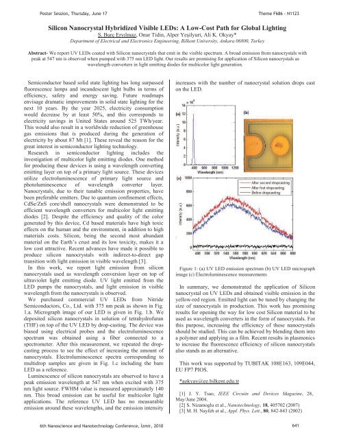
Poster Session, Thursday, June 17Theme F686 - N1123Silicon Nanocrystal Hybridized Visible LEDs: A Low-Cost Path for Global Light<strong>in</strong>gŞ. Burç Eryılmaz, Onur Tid<strong>in</strong>, Alper Yeşilyurt, Ali K. Okyay*Department of Electrical and Electronics Eng<strong>in</strong>eer<strong>in</strong>g, Bilkent University, Ankara 06800, TurkeyAbstract- We report UV LEDs coated with Silicon nano<strong>crystals</strong> that emit <strong>in</strong> the visible spectrum. A broad emission from nano<strong>crystals</strong> withpeak at 547 nm is observed when pumped with 375 nm LED light. Our results are promis<strong>in</strong>g for application of Silicon nano<strong>crystals</strong> aswavelength converters <strong>in</strong> light emitt<strong>in</strong>g diodes for multicolor light generation.Semiconductor based solid state light<strong>in</strong>g has long surpassedfluorescence lamps and <strong>in</strong>candescent light bulbs <strong>in</strong> terms ofefficiency, safety and energy sav<strong>in</strong>g. Future roadmapsenvisage dramatic improvements <strong>in</strong> solid state light<strong>in</strong>g for thenext 10 years. By the year 2025, electricity consumptionwould decrease by at least 50%, and this corresponds toelectricity sav<strong>in</strong>gs <strong>in</strong> United States around 525 TWh/year.This would also result <strong>in</strong> a worldwide reduction of greenhousegas emissions that is produced dur<strong>in</strong>g the generation ofelectricity by about 87 Mt [1]. These reveal the reason for thegreat <strong>in</strong>terest <strong>in</strong> semiconductor light<strong>in</strong>g technology.Research <strong>in</strong> semiconductor light<strong>in</strong>g <strong>in</strong>cludes the<strong>in</strong>vestigation of multicolor light emitt<strong>in</strong>g diodes. One methodfor produc<strong>in</strong>g these devices is us<strong>in</strong>g a wavelength convert<strong>in</strong>gemitt<strong>in</strong>g layer on top of a primary light source. These devicesutilize electrolum<strong>in</strong>escence of primary light source andphotolum<strong>in</strong>escence of wavelength converter layer.Nano<strong>crystals</strong>, due to their tunable emission properties, havebeen preferable emitters. Due to quantum conf<strong>in</strong>ement effects,CdSe/ZnS core/shell nano<strong>crystals</strong> were demonstrated to beefficient wavelength converters for multicolor light emitt<strong>in</strong>gdiodes [2]. Despite the efficiency and quality of the colorgenerated by this device, Cd based materials have high toxiceffects on the human and the environment, <strong>in</strong> addition to highmaterials costs. Silicon, be<strong>in</strong>g the second most abundantmaterial on the Earth’s crust and its low toxicity, makes it alow cost attractive. Recent advances have made it possible toproduce silicon nano<strong>crystals</strong> with <strong>in</strong>direct-to-direct gaptransition with light emission <strong>in</strong> visible wavelength [3].In this work, we report light emission from siliconnano<strong>crystals</strong> used as wavelength conversion layer on top ofultraviolet light emitt<strong>in</strong>g diode. UV light emitted from theLED pumps the nano<strong>crystals</strong>, and light emission <strong>in</strong> visiblewavelength from the nano<strong>crystals</strong> is observed.We purchased commercial UV LEDs from NitrideSemiconductors, Co., Ltd. with 375 nm peak as shown <strong>in</strong> Fig.1.a. Micrograph image of our LED is given <strong>in</strong> Fig. 1.b. Wedeposited silicon nano<strong>crystals</strong> <strong>in</strong> solution of tetrahydrofuran(THF) on top of the UV LED by drop-cast<strong>in</strong>g. The device wasbiased us<strong>in</strong>g electrical probes and the electrolum<strong>in</strong>escencespectrum was obta<strong>in</strong>ed us<strong>in</strong>g a fiber connected to aspectrometer. After this measurement, we repeated the dropcast<strong>in</strong>gprocess to see the effect of <strong>in</strong>creas<strong>in</strong>g the amount ofnano<strong>crystals</strong>. Electrolum<strong>in</strong>escence spectra correspond<strong>in</strong>g tomultidrop samples are given <strong>in</strong> Fig. 1.c <strong>in</strong>clud<strong>in</strong>g the bareLED as a reference.Lum<strong>in</strong>escence of silicon nano<strong>crystals</strong> are observed to have apeak emission wavelength at 547 nm when excited with 375nm light source. FWHM value is measured approximately 140nm. This broad emission can be useful for multicolor lightapplications. The reference UV LED has no measurableemission around these wavelengths, and the emission <strong>in</strong>tensity<strong>in</strong>creases with the number of nanocrystal solution drops caston the LED.Figure 1: (a) UV LED emission spectrum (b) UV LED micrographimage (c) Electrolum<strong>in</strong>escence measurementsIn summary, we demonstrated the application of Siliconnanocrystal on UV LEDs and obta<strong>in</strong>ed visible emission <strong>in</strong> theyellow-red region. Emitted light can be tuned by chang<strong>in</strong>g thesize of nano<strong>crystals</strong> <strong>in</strong> production. This work has promis<strong>in</strong>gresults for open<strong>in</strong>g the way for low cost Silicon material to beused as wavelength converters <strong>in</strong> the form of nano<strong>crystals</strong>. Forthis purpose, <strong>in</strong>creas<strong>in</strong>g the efficiency of these nano<strong>crystals</strong>should be studied. This can be achieved by blend<strong>in</strong>g them <strong>in</strong>toa polymer and apply<strong>in</strong>g as a film. Recent results <strong>in</strong> plasmonicsto <strong>in</strong>crease the fluorescence efficiency of silicon nano<strong>crystals</strong>also stands as an alternative.This work was supported by TUBITAK 108E163, 109E044,EU FP7 PIOS.*aokyay@ee.bilkent.edu.tr[1] J. Y. Tsao, IEEE Circuits and Devices Magaz<strong>in</strong>e, 28,May/June 2004.[2] S. Nizamoglu et al., Nanotechnology, 18, 405702 (2007)[3] M. H. Nayfeh et al., Appl. Phys. Lett., 80, 842-843 (2002)6th Nanoscience and Nanotechnology Conference, zmir, 2010 641


