

Electronics-World-1959-05

You also want an ePaper? Increase the reach of your titles
YUMPU automatically turns print PDFs into web optimized ePapers that Google loves.
ligible. Consequently, the voltage<br />
waveform at the output of the modulator<br />
and on the screen of the 807<br />
consists of positive half -cycles of audio.<br />
This is an important requirement. See<br />
"Transmitter Adjustments."<br />
Tests have shown that the power<br />
output of the 807 buffer on modulation<br />
peaks is four times that of the stage<br />
under conditions of no modulation or<br />
"idling." Also, with proper adjustment<br />
of R, as well as buffer and final amplifier<br />
grid drive (which is quite easily<br />
obtained), the resultant carrier power<br />
is proportional to the voltage change<br />
on the screen of the 807. (Note: This<br />
does not mean that the plate current of<br />
the 807 is also proportional to screen<br />
voltage change.)<br />
Resistor R, provides excellent load for<br />
the output circuit of the modulator. Its<br />
value is fixed at 25,000 ohms and requires<br />
no initial or periodic adjustment.<br />
Also, it will be noted that the resistor<br />
handles a maximum current of only 10<br />
to 13 ma., so that the power rating<br />
need be only 4 watts, and a minimum of<br />
source voltage is required.<br />
Design of R.F. Stages<br />
Conventional input and output circuitry<br />
is employed in buffer and final<br />
amplifier stages, as shown in Fig. 3. Important<br />
design requirements are: (a)<br />
sufficient drive for each stage to provide<br />
recommended operating grid current<br />
values for the type tubes used;<br />
(b) a fixed source of grid bias and<br />
screen supply voltage for the buffer<br />
and final amplifier; (c) complete isolation<br />
of stages to prevent both regenerative<br />
and degenerative feedback; and<br />
(d) provision for r.f. drive adjustment<br />
to both stages. Of course, the plate<br />
supply sources for both stages should<br />
have reasonably good regulation to<br />
prevent peak clipping. Also, the antenna<br />
system to be used with the<br />
transmitter should be capable of loading<br />
the transmitter to at least 75% full<br />
power output. Inadequate antenna<br />
loading results in a lower depth of<br />
modulation than is otherwise obtainable.<br />
The r.f. drive adjustment for the<br />
buffer, and to some extent for the final<br />
amplifier, is provided by the adjustable<br />
grid resistor R. Other methods can be<br />
employed for the purpose, of course,<br />
but if more than ample drive power is<br />
available from the preceding stage, the<br />
adjustable resistor method is particularly<br />
effective; moreover, it has the advantage<br />
of maintaining high efficiency<br />
in the buffer and thus high peak -power<br />
output from the stage. Optimum grid<br />
current values for the final amplifier<br />
can be obtained conveniently by readjustment<br />
of the tuned grid circuit.<br />
In fact, use of the tuned circuit in this<br />
manner is the preferred method of adjusting<br />
the grid current for the final<br />
stage.<br />
One more point should be mentioned<br />
in regard to r.f. design and that is the<br />
advisability of using a slightly higher<br />
"Q" in the plate circuit of the buffer<br />
and in the grid circuit of the final. This<br />
provides better load regulation for the<br />
N<br />
150<br />
LEGEND<br />
R.F DRIVE VARIATIONS<br />
UPWARD AT AUDIO FRED.<br />
I 1<br />
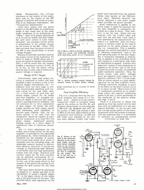
Fig. 4. How r.f. drive to power amplifier pre.<br />
vents p.a. cut -off, and constantly changes<br />
grid operating point at a.f. frequency.<br />
's<br />
r izo<br />
Slo<br />
Ñ T<br />
S<br />
U .<br />
,el 11<br />
5 45 50 55 60<br />
ANTENNA CURRENT<br />
65<br />
CLASS A82<br />
«.GLAS$ ADI<br />
I<br />
FOR<br />
Fig. 5. Actual antenna current values for<br />
several values of buffer screen voltage.<br />
large variations in r.f. current in these<br />
circuits.<br />
Final Amplifier Efficiency<br />
Fig. 6 is a diagram showing the pertinent<br />
elements and values of a 1 kw.<br />
input p.e.p. (peak- envelope -power)<br />
transmitter which is currently being<br />
used by the author on the 80 -, 40- and<br />
20 -meter phone bands. It was originally<br />
a 500 -watt rig, designed and built by<br />
the author in 1950, and utilized a pair<br />
of 803's in the final. QSO reports on the<br />
transmitter were excellent. In 1951 the<br />
803 tubes were replaced by the new<br />
and more efficient 4 -125A type tubes,<br />
Fig. 6. Shown at the<br />
right is the schematic<br />
diagram of the modulator,<br />
buffer, and the<br />
final power amplifier<br />
stage of the one -kilowatt<br />
(peak- envelopepower<br />
input) transmitter<br />
that is employed<br />
by the author. Refer<br />
to the text for a<br />
complete description.<br />
AUDIO FROM<br />
$PEECN AMP<br />
445 V)<br />
807<br />
R F DRIVER<br />
which were operated from the original<br />
clamp tube exciter at the 500 -watt<br />
p.e.p. input. Recently, however, the<br />
author obtained a new plate supply<br />
which provides the power increase.<br />
Since modulation is applied to the<br />
driver stage, it might be assumed that<br />
the final amplifier is necessarily operated<br />
as a class B linear. This, however.<br />
is not the case. Those who are<br />
familiar with the 4 -125A tubes will<br />
note that the grid bias value used is<br />
that specified by the manufacturer for<br />
class C c.w. operation. Also, the transmitter<br />
is initially tuned up for class C<br />
operation in the same manner as for<br />
any c.w. transmitter. This is possible<br />
because the system described is a form<br />
of "efficiency modulation," that is, the<br />
grid operating point of the final amplifier<br />
is constantly changing as modulation<br />
is applied to the preceding driver<br />
and remains at a fixed point only when<br />
no modulation is applied. Another very<br />
important reason is that modulation is<br />
applied to the driver, only in the form<br />
of positive cycles of audio, as explained<br />
under modulator operation. Thus, the<br />
driver screen (and plate) voltages<br />
never go negative with respect to the<br />
fixed d.c. potential ( "B + ") on the stage.<br />
This of course results in a grid operating<br />
point for the final amplifier which,<br />
although constantly changing, is never<br />
so far down on the plate current curve<br />
as to cause cut -off. Observation of the<br />
r.f. modulated waveform on an oscilloscope<br />
shows the negative modulation<br />
peaks to be only a small percentage of<br />
the amplitude of the positive peaks.<br />
See Figs. 4 and 5.<br />
While it is practical to adjust this<br />
system so that the carrier will be near<br />
zero with no modulation, it is not considered<br />
desirable. It can be seen that<br />
the average carrier power will be lower.<br />
Experience with this system of modulation<br />
has indicated that it is preferable<br />
to maintain an unmodulated carrier<br />
(Continued on page 144)<br />
4- 125A'S<br />
FA<br />
375 V (TOTAL CJRRENT 15 MA)<br />
ANT<br />
May. <strong>1959</strong> 61