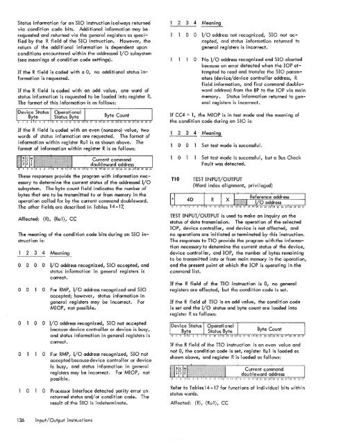
Status information for an S10 instruction isalways returnedvia condition code bits. Additional information may berequested and returned via the general registers as specifiedby the R field of the S10 instruction. However, thereturn of the additional information is dependent uponconditions encountered within the addressed I/O sub<strong>system</strong>(see meanings of condition code settings).If the R field is coded with a 0, no additional status informationis requested.If the R field is coded with an odd value, one word ofstatus information is requested to be loaded into register R.<strong>The</strong> format of this information is as follows:If the R field is coded with an even (nonzero) value, twowords of status information are requested. <strong>The</strong> format ofinformation within register Ru1 is as shown above. <strong>The</strong>format of information within register R is as follows:<strong>The</strong>se responses provide the program with information necessaryto determine the current status of the addressed I/osub<strong>system</strong>. <strong>The</strong> byte count field indicates the number ofbytes that are to be transmitted to or from memory in theoperation called for by the current command doubleword.<strong>The</strong> other fields are described in Tables 14-17.Affected: (R), (Ru1), CC<strong>The</strong> meaning of the condition code bits during an SIO instructionis:2 3 4 Meaningo 0 0 0 I/O address recognized, S10 accepted, andstatus information in general registers iso 0ooocorre~t.o For RMP, I/O address recognized and S10accepted; however, status i nformati on ingeneral registers may be incorrect. ForMIOP, not possible.0 0 I/O address recognized, SIO not acceptedbecause device controller or device is busy,and status information in general registers iscorrect.o For RMP, I/O address recognized, SIO notaccepted because device controller or deviceis busy, and status information in generalregisters may be incorrect. For MIOP, notpossible.o Processor Interface detected parity error onreturned status and/or condition code. <strong>The</strong>result of the SIO is indeterminate.2 3 4 Meaningo 0 I/o address not recognized, SIO not accepted,and status information returned togeneral registers is incorrect.o No I/O address recognized and SIO abortedbecause an error detected when the lOP attemptedto read and transfer the _S10 parameters(device/device controller address, Rfield information, and first command doublewordaddress) from the BP to the lOP via mainmemory. Status information returned to generalregisters is incorrect.If CC4 = 1, the MIOP is in test mode and the meaning ofthe condition code during an SIO is:TID2 3 4 Meaningo 0oSet test mode is successful.Set test mode is successful, but a Bus CheckFault was detected.TEST INPUT/OUTPUT(Word index alignment, privileged)TEST INPUT/OUTPUT is used to make an inquiry on thestatus of data transmission. <strong>The</strong> operation of the selectedlOP, device controller, and device is not affected, andno operations are initiated or terminated by this instruction.<strong>The</strong> responses to no provide the program with the informationnecessary to determine the current status of the device,device controller, and lOP, the number of bytes remainingto be transmitted into or from main memory in the operation,and the present point at which the lOP is operating in thecommand list.If the R field of the no instruction is 0, no generalregisters are affected, but the condition code is set.If the R field of no is an odd value, the condition codeis set and the I/o status and byte count are loaded intoregister R as follows:If the R field of the no instruction is an even value andnot 0, the condition code is set, register Ru1 is loaded asshown above, and register R is loaded as follows:Refer to Tables 14 -17 for functions of individual bits withinstatus words.Affected: (R), (Ru1), CC136 Input/Output Instructions
If CC4 = 0, the MIOP is in a normal mode of operation andthe meaning of the condition code during a no is:TDVTEST DEVICE(Word index alignment, privileged)2 3 4 Meaning000o 0o 0oo I/O address recognized, acceptable SIO iscurrently possible, and status information ingeneral registers is correct.o For RMP, I/O address recognized, acceptableSIO is currently possible; however, statusinformation in the general registers may beincorrect. For MIOP, not possible.o I/o address recognized but acceptable SIOis not currently possible because device controlleror device is busy. Status informationin general registers is correct.o For RMP, I/O address recognized but acceptableSIO is not currently possible becausedevice controller or device is busy; statusinformation in general registers may be incorrect.For MIOP, not possible.TEST DEVICE is used to provide information about a deviceother than that obtainable by means of the no instruction.<strong>The</strong> operation of the selected lOP, device controller, anddevice is not affected, and no operations are initiated orterminated. <strong>The</strong> responses to TDV provide the program withinformation giving details on the condition of the selecteddevice, the number of bytes remaining to be transmitted inthe current operation, and the present point at which thelOP is operating in the command list.If the R field of the TDV instruction is 0, the conditioncode is set, but no general registers are affected.If the R field of TDV is an odd value, the condition codeis set and the device status and byte count are loaded intoregister R as follows:oo 0o Processor Interface detected parity error onreturned status and/or condition code. <strong>The</strong>result of the no is indeterminate.I/O address not recognized, no not accepted,and status information returned togeneral registers is incorrect .If the value of the R field of TDV is an even value andnot 0, the condition code is set, register Ru1 is loaded asshown above, and register R is loaded as follows:o..... 1_ T Ir. _...<strong>1.</strong>..1__________ : __ ...1 __...I TTr. _L... __ ~_.J.'v <strong>1.</strong>/ '-' \,oiu ...... C;~ • C,"",~III~vU ..... I.U .... '"" ......,va ."""'"because an error detected when the lOP attemptedto read and transfer the no parameters(device/device controller address andR field information) from the BP to the lOP viamain memory. Status information returned togeneral registers is incorrect.If CC4 = 1, the MIOP is in the test mode and the meaningof the condition code during a no is:2 3 4 Meaning000o 0o 0Unit is performing an Order Out operation.Unit is performing an Order In operation.Unit is performing a Data Out operation.D_C __ ~_ ~L... __ ~_I: __ L...I~ ~""r:_L...""r_1 r""&",,ro ... _o .... ,.. ..... ,..1 &,..r""'''' 'v "'" "'"t't""""'"~'" t"'" 't""""~' ''', .... "" ... " .. ,-,,--, ''''description of Device Status Byte. Refer to Tables 16 and 17for functions of other bits within status words.Affected: (R), (Ru 1), CCIf CC4 = 0, the MIOP is in a normal mode of operation andthe meaning of the condition code during a TDV is:2 3 4 Meaningo 0 0 0 I/O address recognized, no device-dependentcondition present, and status information ingeneral registers is correct.o 0o For RMP, I/O address recognized and nodevice-dependent condition present; however,status information in general registers may beincorrect. For MIOP, not possible.oParity error detected by Processor Interfaceon returned status and/or condition code.<strong>The</strong> result of the no is indeterminate.oo 0I/O address recognized and device-dependentcondition is present or device controller is intest mode.oUnit is performing a Data In operation.BCF detected while unit performing a DataIn operati on.oo For RMP, I/o address recognized, devicedependentcondition is present, or device controlleris in test mode; but status informationin the general registers may be incorrect. ForMIOP, not possible.Input/Output Instructions 137
- Page 1 and 2:
Xerox 560 ComputerReference Manual9
- Page 5 and 6:
4. INPUT/OUTPUT OPERA TIO NS 142 AG
- Page 7 and 8:
1. XEROX 560 COMPUTER SYSTEMINTRODU
- Page 10 and 11:
Many operations are performed in fl
- Page 12 and 13:
Rapid Context Switching. When respo
- Page 14 and 15:
2. SYSTEM ORGANIZATIONThe elements
- Page 16:
FAST MEMORYARITHMETIC AND CONTROL U
- Page 19 and 20:
INFORMATION BOUNDARIESBasic process
- Page 21 and 22:
(Maximumof eight)Core Core Core Cor
- Page 23 and 24:
3. Diagnostic logic. Each memory dr
- Page 25 and 26:
eference address field of the instr
- Page 27 and 28:
Instruction in memory:Instruction i
- Page 29 and 30:
Real-extended addressing is specifi
- Page 31:
Table 1. Basic Processor Operating
- Page 35 and 36:
DesignationFunctionDesignationFunct
- Page 37 and 38:
InterruptStateDisarmedArmed[$Waitin
- Page 39 and 40:
AddressTable 2. Interrupt Locations
- Page 41 and 42:
is assumed to contain an XPSD or a
- Page 43 and 44:
Table 3. Summary of Trap LocationsL
- Page 45 and 46:
TRAP MASKSThe programmer may mask t
- Page 47 and 48:
PUSH-DOWN STACK LIMIT TRAPPush-down
- Page 49 and 50:
Instruction Name Mnemonic FaultDeci
- Page 51 and 52:
subroutine. However, with certain c
- Page 53 and 54:
3. INSTRUCTION REPERTOIREThis chapt
- Page 55 and 56:
CC1 is unchanged by the instruction
- Page 57 and 58:
Condition code settings:2 3 4 Resul
- Page 59 and 60:
Example 2, odd R field value:Before
- Page 61 and 62:
significance (FS), floating zero (F
- Page 63 and 64:
next sequential register after regi
- Page 65 and 66:
R 1 R2 R3 MeaningoThe effective vir
- Page 67 and 68:
Condition code settings:2 3 4 Resul
- Page 69 and 70:
MIMULTIPLY IMMEDIATE(Immediate oper
- Page 71 and 72:
original contents of register R, re
- Page 73 and 74:
Instruction NameCompare HalfwordMne
- Page 75 and 76:
Condition code settings:2 3 4 Resul
- Page 77 and 78:
2 3 4 Result of ShiftCircular Shift
- Page 79 and 80:
4. At the completion of the left sh
- Page 81 and 82:
Instruction NameFloating Subtract L
- Page 83 and 84:
The following table shows the possi
- Page 85 and 86:
Table 8.Condition Code Settings for
- Page 87 and 88:
PACKED DECIMAL NUMBERSAll decimal a
- Page 89 and 90:
DSTDECIMAL STORE(Byte index alignme
- Page 91 and 92: If no indirect addressing or indexi
- Page 93 and 94: Instruction NameMnemonicDesignation
- Page 95 and 96: Both byte strings are C bytes in le
- Page 97 and 98: of the destination byte that caused
- Page 99 and 100: again present, unti I a positive or
- Page 101 and 102: The new contents of register 7 are:
- Page 103 and 104: traps to location X'42 1 as a resul
- Page 105 and 106: If there is sufficient space in the
- Page 107 and 108: If CC1, or CC3, or both CC1 and CC3
- Page 109 and 110: appropriate memory stack locations
- Page 111 and 112: II, EI) are generated by II ORing"
- Page 113 and 114: In the real extended addressing mod
- Page 115 and 116: CAll INSTRUCTIONSEach ofthe four CA
- Page 117 and 118: The XPSD instruction' is used for t
- Page 119 and 120: If (I)1O = 0, trap or interrupt ins
- Page 121 and 122: For either memory map format and ei
- Page 123 and 124: initial value plus the initial valu
- Page 125 and 126: Table 9. Status Word 0Field Bits Co
- Page 127 and 128: READ INTERRUPT INHIBITSThe followin
- Page 129 and 130: Table 11.Read Direct Mode 9 Status
- Page 131 and 132: SET ALARM INDICATORThe following co
- Page 133 and 134: INPUT jOUTPUT INSTRUCTIONSThe I/o i
- Page 135 and 136: Table 13.Description of I/o Instruc
- Page 137 and 138: Table 15.Device Status Byte (Regist
- Page 139 and 140: Table 16. Operational Status Byte (
- Page 141: Table 19.Status Response Bits for A
- Page 145 and 146: 2 3 4 Meaningo 0 I/o address not re
- Page 147 and 148: The functions of bits within the DC
- Page 149 and 150: 4. Each unit-record controller (int
- Page 151 and 152: Interrupt at Channel End (Bit Posit
- Page 153 and 154: Transfer in Channel. A control lOCO
- Page 155 and 156: Otherwise, the first word of the ne
- Page 157 and 158: Depending upon the characteristics
- Page 159 and 160: change the rate on the primary cons
- Page 161 and 162: Location(hex) (dec)20 3221 3322 342
- Page 163 and 164: Table 22.Diagnostic Control (P-Mode
- Page 165 and 166: at its normal rate (e. g., fixed du
- Page 167 and 168: SET LOW CLOCK MARGINSThis command c
- Page 169 and 170: BP STATUS AND NO.Th i s group of i
- Page 171 and 172: Input5MPri ntout5MFunctionStore X 1
- Page 173 and 174: 6. SYSTEM CONFIGURATION CONTROLPool
- Page 175 and 176: Table 25. Functions of Processor Cl
- Page 177: Table 26. Functions of Memory Unit
- Page 180 and 181: STANDARD 8-BIT COMPUTER CODES (EBCD
- Page 182 and 183: STANDARD SYMBOL-CODE CORRESPONDENCE
- Page 184 and 185: STANDARD SYMBOL-CODE CORRESPONDENCE
- Page 186 and 187: TABLE OF POWERS OF SIXTEEN II162564
- Page 188 and 189: HEXADECIMAL-DECIMAL INTEGER CONVERS
- Page 190 and 191: HEXADECIMAL-DECIMAL INTEGER CONVERS
- Page 192 and 193:
HEXADECIMAL-DECIMAL INTEGER CONVERS
- Page 194 and 195:
HEXADECIMAL-DECIMAL FRACTION CONVER
- Page 196 and 197:
HEXADECIMAL-DECIMAL FRACTION CONVER
- Page 198 and 199:
APPENDIX B.GLOSSARY OF SYMBOLIC TER
- Page 200 and 201:
TermMeaningTermMeaningWKxWrite key
- Page 202 and 203:
Table C-2. Memory Unit Status Regis
- Page 204 and 205:
Y OYf'lV r'f'lrnf'lrtil"\n'''' ....
- Page 206:
701 South Aviation BoulevardEI Segu