11-bit page address in the accessed element of the memorymap array replaces the 8 high-order bits of the virtual addressto produce the actual address of the main memory locationto be used by the instruction (20-bit word addressthat is automatically adjusted as required for doubleword,halfword, or byte operation). See Figure 7.Note: If the 11-bit page address in the accessed elementof the memory map is all zeros, and an actual addressis produced that corresponds to a word addressin the range 0 through 15, when the ll-bit pageaddress is combined with the 9 low-order bits of thevirtual address, the corresponding general registerin the current register block is not accessed. Inthis one particular instance a word address in therange 0 through 15 corresponds to an actual mainmemory location rather than a general register.REAL MEMORY WRITE LOCKSAdditional memory protection, independent of the accessprotection, is provided by a write lock and key technique.A 4-bit write protect lock (WL) is provided for each 512-word page of actual memory. Thus, for the maximum 1Mwordreal memory there would be 2048 4-bit write locks.Write locks are assigned to pages of actual addresses asfollows:Actual addressesX'6oo '-X'7FF'Actual addressesX'400'-X'5FF'Actual addressesX'200'-X'3FF'Actual addressesO-X'l FF'(memory page 0)ActualaddressesX'1FEoo'X'l FFFF'(memorypage 255)ActualaddressesX'1FCOO'X' 1FDFF'2. A key value of 0000 is a "skeleton II key that will openany lock; thus write access to any memory page is permittedindependent of its lock value.3. A lock value other than 0000 for a memory page permitswrite access to that page only if the key value(other than 0000) is identical to.the lock value.Thus a program can write into a given memory page if thelock value is 0000, if the key value is 0000, or if the keyvalue matches the lock value.Note: <strong>The</strong> memory access protection feature operates duringvirtualaddressingmodes and on virtual addresses,whereas the memory write protection feature alwaysoperates on actua I memory addresses. Thus, if thememory access protection feature is invoked (thatis, if the basic processor is operating in the slavemode or the master-protected inode and is usi ng thememory map), the access protection codes are examinedwhen the virtual address is converted intoan actual address. <strong>The</strong>n the lock and key are examinedto determine whether the program (master,master-protected, or slave mode) is allowed to alterthe contents of the main memory location correspondingto the final actual address. If an instruction attemptsto write into a write-protected memory page,the basic processor aborts the instruction, and trapsto location X 140 1 , the "nonallowed operation" trap(see "Trap System ", later in this chapter). If anI/O procedure attempts to write into a writeprotectedmemory page, the write lock violation bitin the lOP sta tus byte is set, and can be tested bythe AIO, TIO, and TDV instructions.PROGRAM STATUS WORDS<strong>The</strong> critical control conditions of the basic processor are definedwithin 64 bits of information collectively referred toas the program status words (PSWs). <strong>The</strong> current PSWs maybe considered as one 64-bit internal basic processor register,although they actually exist as a collection of separate registersand flip-flops (see Figure 2 appearing earlier in thischapter). When stored in memory, the PSWs have the followingformat:<strong>The</strong> write protect locks can be changed only by executingthe privileged instruction MOVE TO MEMORY CONTROL(see Chapter 3, "Control Instructions").<strong>The</strong> write key (a 4-bit field in the PSWs for any operatingprogram, or in the command doubleword for I/o operations)works in conjunction with the write lock to determinewhether any program (slave, master-protected, or mastermode) can write into a specific page of main memory iocations.<strong>The</strong> write key and lock control access for writingaccording to these rules:<strong>The</strong>y may be optionally followed by an additional two wordswith the following format:<strong>1.</strong> A lock value of 0000 means that the correspondingmemory page is unlocked; write access to that page ispermitted independent of the key value.28 Main Memory
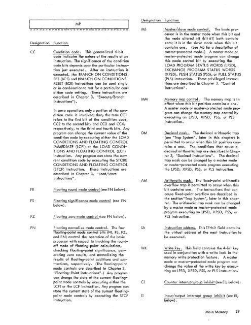
DesignationFunctionDesignationFunctionCC Condition code. This generalized 4-bitcode indicates the nature of the results of aninstruction. <strong>The</strong> significance of the conditioncode bits depends upon the particular instructionjust executed. After an instruction isexecuted, the BRANCH ON CONDITIONSSET (BCS) and BRANCH ON CONDITIONSRESET (BCR) instructions can be used singlyor in combination to test for a particular conditioncode setting. (<strong>The</strong>se instructions aredescribed in Chapter 3, "Execute/BranchInstructions") •FRFSFZIn some operations onlya portion of the conditioncode is involved; thus, the term CC 1refers to the first bit of the condition code,CC2 to the second bit, and CC3 and CC4,respectively, to the third and fourth bits. Anyprogram can change the current value of thecondition code by executing either the LOADCONDITIONS AND FLOATING CONTROLIMMEDIATE (LCFI) or the LOAD CONDITIONS AND FLOATING CONTROL (LCF)instruction. Any program can store the currentcondition code by executing the STORECONDITIONS AND FLOATING CONTROL(STCF) instruction. <strong>The</strong>se instructions aredescribed in Chapter 3, ;;Load/~toreInstructions" .Floating round mode control (see FN below).Floating significance mode control (see FNbelow).Floating zero mode control (see FN below).MS Master/slave mode control. <strong>The</strong> basic processoris in the master mode when this bit andthe mode altered bit (bit 61) both containzero; it is in the slave mode when this bitcontains one. (See MS for a description ofmaster-protected mode.) A master mode ormaster-protected mode program can changethis mode control bit by executing theLOAD PROGRAM STATUS WORDS (LPSD),EXCHANGE PROGRAM STATUS WORDS(XPSD), PUSH STATUS (PSS), or PULL STATUS(PLS) instruction. <strong>The</strong>se privi leged instructionsare described in Chapter 3, "ControlInstructions" •MM Memory map control. <strong>The</strong> memory map is ineffect when this bit position contains a one.A master mode or master-protected mode programcan change the· memory map control byexecuting an LPSD, XPSD, PSS, or PLSinstruction.DM Decimal mask. <strong>The</strong> decimal arithmetic trap(see "Trap System", later in this chapter) ispermitted to occur when this bit position containsa one. <strong>The</strong> conditions that cause adecimal arithmetic trap are described in Chapter3, II Decimal Instructions". <strong>The</strong> decimaltrap mask can be changed by a master modeor master-protected mode program executingthe LPSD, XPSD, PSS, or PLS instruction.AMArithmetic mask. <strong>The</strong> fixed-point arithmeticoverflow trap is permitted to occur when thisbit contains one. <strong>The</strong> instructions that cancause fixed-point overflow are described inthe section "Trap System", later in this chapter.<strong>The</strong> arithmetic trap mask can be changedby a master mode or master-protected modeprogram executing an LPSD, XPSD, PSS, orPLS instruction.FNFloating normalize mode control. <strong>The</strong> fourfloating-point mode control bits (FR, FS, FZ,and FN) control the operation of the basicprocessor with respect to invoking the roundoffmode of floating-point calculations,checking floating-point significance, generatingzero results, and normalizing theresults of floating-point additions and subtractions,respectively. (<strong>The</strong> floating-pointmode controls are described in Chapter 3,"Floating-Point Instructions".) Any programcan change the state of the current floatingpointmode controls by executing either theLCFI or the LCF instruction. Any program canstore the current state of the current floatingpointmode controls by executing the STCFinstruction.IAWKCIIIInstruction address. This 17-bit field containsthe virtual address of the next instruction tobe executed.Write key. This field contains the 4-bit keyused in conjunction with a write lock in thememory write protection feature. A mastermode or master-protected mode program canchange the value of the write key by executingan LPSD, XPSD, PSS, or PLS instruction.Counter interrupt group inhibit (see EI, below).Input/output interrupt group inhibit (see EI,below).Main Memory 29
- Page 1 and 2: Xerox 560 ComputerReference Manual9
- Page 5 and 6: 4. INPUT/OUTPUT OPERA TIO NS 142 AG
- Page 7 and 8: 1. XEROX 560 COMPUTER SYSTEMINTRODU
- Page 10 and 11: Many operations are performed in fl
- Page 12 and 13: Rapid Context Switching. When respo
- Page 14 and 15: 2. SYSTEM ORGANIZATIONThe elements
- Page 16: FAST MEMORYARITHMETIC AND CONTROL U
- Page 19 and 20: INFORMATION BOUNDARIESBasic process
- Page 21 and 22: (Maximumof eight)Core Core Core Cor
- Page 23 and 24: 3. Diagnostic logic. Each memory dr
- Page 25 and 26: eference address field of the instr
- Page 27 and 28: Instruction in memory:Instruction i
- Page 29 and 30: Real-extended addressing is specifi
- Page 31: Table 1. Basic Processor Operating
- Page 37 and 38: InterruptStateDisarmedArmed[$Waitin
- Page 39 and 40: AddressTable 2. Interrupt Locations
- Page 41 and 42: is assumed to contain an XPSD or a
- Page 43 and 44: Table 3. Summary of Trap LocationsL
- Page 45 and 46: TRAP MASKSThe programmer may mask t
- Page 47 and 48: PUSH-DOWN STACK LIMIT TRAPPush-down
- Page 49 and 50: Instruction Name Mnemonic FaultDeci
- Page 51 and 52: subroutine. However, with certain c
- Page 53 and 54: 3. INSTRUCTION REPERTOIREThis chapt
- Page 55 and 56: CC1 is unchanged by the instruction
- Page 57 and 58: Condition code settings:2 3 4 Resul
- Page 59 and 60: Example 2, odd R field value:Before
- Page 61 and 62: significance (FS), floating zero (F
- Page 63 and 64: next sequential register after regi
- Page 65 and 66: R 1 R2 R3 MeaningoThe effective vir
- Page 67 and 68: Condition code settings:2 3 4 Resul
- Page 69 and 70: MIMULTIPLY IMMEDIATE(Immediate oper
- Page 71 and 72: original contents of register R, re
- Page 73 and 74: Instruction NameCompare HalfwordMne
- Page 75 and 76: Condition code settings:2 3 4 Resul
- Page 77 and 78: 2 3 4 Result of ShiftCircular Shift
- Page 79 and 80: 4. At the completion of the left sh
- Page 81 and 82: Instruction NameFloating Subtract L
- Page 83 and 84:
The following table shows the possi
- Page 85 and 86:
Table 8.Condition Code Settings for
- Page 87 and 88:
PACKED DECIMAL NUMBERSAll decimal a
- Page 89 and 90:
DSTDECIMAL STORE(Byte index alignme
- Page 91 and 92:
If no indirect addressing or indexi
- Page 93 and 94:
Instruction NameMnemonicDesignation
- Page 95 and 96:
Both byte strings are C bytes in le
- Page 97 and 98:
of the destination byte that caused
- Page 99 and 100:
again present, unti I a positive or
- Page 101 and 102:
The new contents of register 7 are:
- Page 103 and 104:
traps to location X'42 1 as a resul
- Page 105 and 106:
If there is sufficient space in the
- Page 107 and 108:
If CC1, or CC3, or both CC1 and CC3
- Page 109 and 110:
appropriate memory stack locations
- Page 111 and 112:
II, EI) are generated by II ORing"
- Page 113 and 114:
In the real extended addressing mod
- Page 115 and 116:
CAll INSTRUCTIONSEach ofthe four CA
- Page 117 and 118:
The XPSD instruction' is used for t
- Page 119 and 120:
If (I)1O = 0, trap or interrupt ins
- Page 121 and 122:
For either memory map format and ei
- Page 123 and 124:
initial value plus the initial valu
- Page 125 and 126:
Table 9. Status Word 0Field Bits Co
- Page 127 and 128:
READ INTERRUPT INHIBITSThe followin
- Page 129 and 130:
Table 11.Read Direct Mode 9 Status
- Page 131 and 132:
SET ALARM INDICATORThe following co
- Page 133 and 134:
INPUT jOUTPUT INSTRUCTIONSThe I/o i
- Page 135 and 136:
Table 13.Description of I/o Instruc
- Page 137 and 138:
Table 15.Device Status Byte (Regist
- Page 139 and 140:
Table 16. Operational Status Byte (
- Page 141 and 142:
Table 19.Status Response Bits for A
- Page 143 and 144:
If CC4 = 0, the MIOP is in a normal
- Page 145 and 146:
2 3 4 Meaningo 0 I/o address not re
- Page 147 and 148:
The functions of bits within the DC
- Page 149 and 150:
4. Each unit-record controller (int
- Page 151 and 152:
Interrupt at Channel End (Bit Posit
- Page 153 and 154:
Transfer in Channel. A control lOCO
- Page 155 and 156:
Otherwise, the first word of the ne
- Page 157 and 158:
Depending upon the characteristics
- Page 159 and 160:
change the rate on the primary cons
- Page 161 and 162:
Location(hex) (dec)20 3221 3322 342
- Page 163 and 164:
Table 22.Diagnostic Control (P-Mode
- Page 165 and 166:
at its normal rate (e. g., fixed du
- Page 167 and 168:
SET LOW CLOCK MARGINSThis command c
- Page 169 and 170:
BP STATUS AND NO.Th i s group of i
- Page 171 and 172:
Input5MPri ntout5MFunctionStore X 1
- Page 173 and 174:
6. SYSTEM CONFIGURATION CONTROLPool
- Page 175 and 176:
Table 25. Functions of Processor Cl
- Page 177:
Table 26. Functions of Memory Unit
- Page 180 and 181:
STANDARD 8-BIT COMPUTER CODES (EBCD
- Page 182 and 183:
STANDARD SYMBOL-CODE CORRESPONDENCE
- Page 184 and 185:
STANDARD SYMBOL-CODE CORRESPONDENCE
- Page 186 and 187:
TABLE OF POWERS OF SIXTEEN II162564
- Page 188 and 189:
HEXADECIMAL-DECIMAL INTEGER CONVERS
- Page 190 and 191:
HEXADECIMAL-DECIMAL INTEGER CONVERS
- Page 192 and 193:
HEXADECIMAL-DECIMAL INTEGER CONVERS
- Page 194 and 195:
HEXADECIMAL-DECIMAL FRACTION CONVER
- Page 196 and 197:
HEXADECIMAL-DECIMAL FRACTION CONVER
- Page 198 and 199:
APPENDIX B.GLOSSARY OF SYMBOLIC TER
- Page 200 and 201:
TermMeaningTermMeaningWKxWrite key
- Page 202 and 203:
Table C-2. Memory Unit Status Regis
- Page 204 and 205:
Y OYf'lV r'f'lrnf'lrtil"\n'''' ....
- Page 206:
701 South Aviation BoulevardEI Segu