- Page 1 and 2:
BSIM3v3.2.2 MOSFET ModelUsers’ Ma
- Page 5 and 6:
Table of ContentsCHAPTER 1: Introdu
- Page 7 and 8:
CHAPTER 6: Parameter Extraction 6-1
- Page 9 and 10:
APPENDIX C: References C-1APPENDIX
- Page 11 and 12:
CHAPTER 1: Introduction1.1 General
- Page 14 and 15:
Non-Uniform Doping and Small Channe
- Page 16 and 17:
Non-Uniform Doping and Small Channe
- Page 18 and 19:
Non-Uniform Doping and Small Channe
- Page 20 and 21:
Non-Uniform Doping and Small Channe
- Page 22 and 23:
Non-Uniform Doping and Small Channe
- Page 24 and 25:
Non-Uniform Doping and Small Channe
- Page 26 and 27:
Non-Uniform Doping and Small Channe
- Page 28 and 29:
Mobility Modelµeffµ=01 + ( E E )e
- Page 30 and 31:
Bulk Charge Effectµ eff Ev = , E <
- Page 32 and 33:
Strong Inversion Drain Current (Lin
- Page 34 and 35:
Strong Inversion Current and Output
- Page 36 and 37:
Strong Inversion Current and Output
- Page 38 and 39:
Strong Inversion Current and Output
- Page 40 and 41:
Strong Inversion Current and Output
- Page 42 and 43:
Subthreshold Drain CurrentV1 PSCBE2
- Page 44 and 45:
Effective Channel Length and Widthd
- Page 46 and 47:
Poly Gate Depletion EffectNgateFigu
- Page 48 and 49:
Poly Gate Depletion Effect1.00Tox=8
- Page 50 and 51:
Poly Gate Depletion EffectBSIM3v3.2
- Page 52 and 53:
Poly Gate Depletion Effect2-40 BSIM
- Page 54 and 55:
Unified Channel Charge Density Expr
- Page 56 and 57:
Unified Channel Charge Density Expr
- Page 58 and 59:
Unified Mobility Expression∆QVF(
- Page 60 and 61:
Unified Linear Current ExpressionI=
- Page 62 and 63:
Unified Vdsat ExpressionLet V ds =V
- Page 64 and 65:
Single Current Expression for All O
- Page 67 and 68:
KAPITEL 7RESULTAT OCH REKOMMENDATIO
- Page 69 and 70:
CHAPTER 4: Capacitance ModelingAccu
- Page 71 and 72:
Geometry Definition for C-V Modelin
- Page 73 and 74:
Methodology for Intrinsic Capacitan
- Page 75 and 76:
Methodology for Intrinsic Capacitan
- Page 77 and 78:
Methodology for Intrinsic Capacitan
- Page 79 and 80:
Methodology for Intrinsic Capacitan
- Page 81 and 82:
Methodology for Intrinsic Capacitan
- Page 83 and 84:
Charge-Thickness Capacitance Modelp
- Page 85 and 86:
Charge-Thickness Capacitance Modelw
- Page 87 and 88:
Extrinsic CapacitanceFigure 4-4 ill
- Page 89 and 90:
Extrinsic Capacitance2( V + δ ) 4
- Page 91 and 92:
CHAPTER 5: Non-Quasi Static Model5.
- Page 93 and 94:
Model FormulationFigure 5-1. Quasi-
- Page 95 and 96:
Model Formulationwhere elm is the E
- Page 97 and 98:
Model Formulationwhere i represents
- Page 99 and 100:
CHAPTER 6: Parameter ExtractionPara
- Page 101 and 102:
Extraction ProcedureWOrthogonal Set
- Page 103 and 104:
Extraction ProcedureInitial Guess o
- Page 105 and 106:
Extraction Procedureoptimization. (
- Page 107 and 108:
Extraction ProcedureStep 7Extracted
- Page 109 and 110:
Extraction ProcedureB0, B1Fitting T
- Page 111 and 112:
Extraction ProcedureStep 20Extracte
- Page 113 and 114:
Notes on Parameter Extraction6.4.2
- Page 115 and 116:
Notes on Parameter ExtractionnC-1.
- Page 117 and 118:
CHAPTER 6: Parameter ExtractionPara
- Page 119 and 120:
Extraction ProcedureWOrthogonal Set
- Page 121 and 122:
Extraction ProcedureInitial Guess o
- Page 123 and 124:
Extraction Procedureoptimization. (
- Page 125 and 126:
Extraction ProcedureStep 7Extracted
- Page 127 and 128:
Extraction ProcedureB0, B1Fitting T
- Page 129 and 130:
Extraction ProcedureStep 20Extracte
- Page 131 and 132:
Notes on Parameter Extraction6.4.2
- Page 133 and 134:
Notes on Parameter ExtractionnC-1.
- Page 135 and 136:
CHAPTER 7: Benchmark Test ResultsA
- Page 137 and 138:
Benchmark Test ResultsIds (A)1.E-02
- Page 139 and 140:
Benchmark Test ResultsIds (A)1.E-03
- Page 141 and 142:
Benchmark Test Resultsgm/Ids (mho/A
- Page 143 and 144:
Benchmark Test ResultsIds (A)8.E-05
- Page 145 and 146:
CHAPTER 8: Noise Modeling8.1 Flicke
- Page 147 and 148:
Flicker NoiseNlC=ox( V −V− min(
- Page 149 and 150: Noise Model Flag8.3 Noise Model Fla
- Page 151 and 152: CHAPTER 9: MOS Diode Modeling9.1 Di
- Page 153 and 154: Diode IV ModelJssw= Js0sw⎛ E⎜
- Page 155 and 156: MOS Diode Capacitance Model9.1.3 Mo
- Page 157 and 158: MOS Diode Capacitance Model(9.18)Cj
- Page 159 and 160: MOS Diode Capacitance Model(9.26)Cj
- Page 161 and 162: MOS Diode Capacitance Model(9.32)
- Page 163 and 164: APPENDIX A: Parameter ListA.1 Model
- Page 165 and 166: DC ParametersSymbolsused inequation
- Page 167 and 168: DC ParametersSymbolsused inequation
- Page 169 and 170: C-V Model ParametersSymbolsused ine
- Page 171 and 172: dW and dL ParametersA.5 dW and dL P
- Page 173 and 174: Temperature ParametersSymbolsused i
- Page 175 and 176: Process ParametersSymbolsused inequ
- Page 177 and 178: Model Parameter NotesK2( γ1−γ)(
- Page 179 and 180: Model Parameter NotesCgdo = dlc * C
- Page 181 and 182: APPENDIX B: Equation ListB.1 I-V Mo
- Page 183 and 184: I-V ModelC C V C V D L effDL effdsc
- Page 185 and 186: I-V ModelEsatsat= 2νµ effB.1.5 Ef
- Page 187 and 188: I-V ModelB.1.8 Polysilicon Depletio
- Page 189 and 190: Capacitance Model EquationsTRdsw( T
- Page 191 and 192: Capacitance Model EquationsB.2.2.2
- Page 193 and 194: Capacitance Model EquationsQ inv= 0
- Page 195 and 196: Capacitance Model Equationsif (V ds
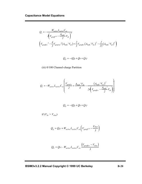
- Page 197 and 198: Capacitance Model Equations⎡Q W L
- Page 199: Capacitance Model EquationsVgsteff
- Page 203 and 204: Capacitance Model EquationsAbulk0
- Page 205 and 206: Capacitance Model Equations(3) capM
- Page 207 and 208: Capacitance Model EquationsδQsub=
- Page 209 and 210: APPENDIX C: References[1] G.S. Gild
- Page 211 and 212: [18] M.C. Jeng, "Design and Modelin
- Page 213 and 214: [35] K.K. Hung et al, “A Physics-
- Page 215 and 216: APPENDIX D: Model Parameter Binning
- Page 217 and 218: DC ParametersSymbolsused inequation
- Page 219 and 220: DC ParametersSymbolsused inequation
- Page 221 and 222: AC and Capacitance ParametersD.3 AC
- Page 223 and 224: NQS ParametersD.4 NQS ParametersSym
- Page 225 and 226: Temperature ParametersD.6 Temperatu
- Page 227 and 228: Process ParametersSymbolsused inequ