STX Signal Transmitter Installation and Operation ... - Kistler-Morse
STX Signal Transmitter Installation and Operation ... - Kistler-Morse
STX Signal Transmitter Installation and Operation ... - Kistler-Morse

Create successful ePaper yourself
Turn your PDF publications into a flip-book with our unique Google optimized e-Paper software.
Chapter 3. St<strong>and</strong>-Alone <strong>STX</strong> Analog Calibration <strong>and</strong> Setup<br />
Amplifier Gain<br />
Adjusting the amplifier gain increases or<br />
decreases system sensitivity. The type of<br />
sensors connected to the <strong>STX</strong> determines<br />
the required gain. For example, for a nominal<br />
excitation output of 12 volts, the reference<br />
voltage is one quarter of the excitation<br />
voltage, or 3 volts. At a gain of 1, the A/D<br />
converter spreads 2,097,152 counts over a<br />
range of ± 3 volts. A gain of 2 spreads the<br />
counts over a range of ± 1.5 volts, doubling<br />
the sensitivity. A gain of 4 spreads the counts<br />
over a range of ± 0.75 volts, doubling the<br />
sensitivity again, etc.<br />
The default gain is 2, appropriate for K-M<br />
Microcell <strong>and</strong> L-Cell sensors. A gain<br />
of 4 is appropriate for K-M Load Disc II,<br />
Load St<strong>and</strong> II, <strong>and</strong> Load Link I <strong>and</strong> II sensors.<br />
Refer to Table 3-4 for the positions of DS1<br />
through DS8 <strong>and</strong> then follow the procedure in<br />
Setting Up the Parameter.<br />
DS4 DS3 DS2 DS1 Amplifier Sensor Input<br />
Gain Voltage<br />
x 0 0 0 2* ±1.5<br />
x 0 0 1 1 ±3.0<br />
x 0 1 0 4 ±0.75<br />
x 0 1 1 8 ±0.375<br />
x 1 0 0 16 ±0.1875<br />
x 1 0 1 32 ±0.09375<br />
x 1 1 0 64 ±0.046875<br />
x 1 1 1 128 ±0.0234375<br />
1 = on, 0 = off, x = does not matter, * = default<br />
Note: To select Amplifier Gain, set dipswitches DS5<br />
through DS8: DS8 = 0, DS7 = 0, DS6 = 0, DS5 = 1.<br />
Table 3-4. Amplifier Gain Dipswitch Settings<br />
Effective Resolution<br />
This parameter controls effective resolution<br />
by changing the conversion rate of the 21-bit<br />
A/D converter. In general, the higher the<br />
resolution, the slower the <strong>STX</strong> conversion<br />
time but the greater the stability.<br />
Refer to Table 3-5 for the positions of DS1<br />
through DS8 <strong>and</strong> then follow the procedure in<br />
Setting Up the Parameter.<br />
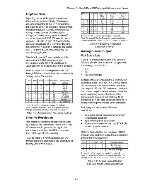
DS4 DS3 DS2 DS1 Effective Conversion Conversion<br />
Res. Time Rate<br />
(bits) (mS) (Conv/s)<br />
x 0 0 0 21 512 2<br />
x 0 0 1 20 250 4*<br />
x 0 1 0 19 125 8<br />
x 0 1 1 18 83 12<br />
x 1 0 0 17 50 20<br />
x 1 0 1 16 25 40<br />
1 = on, 0 = off, x = does not matter, * = default<br />
Note: To select Effective Resolution, set dipswitches<br />
DS5 through DS8: DS8 = 0, DS7 = 0, DS6 = 1, DS5 = 0.<br />
Table 3-5. Effective Resolution<br />
Dipswitch Settings<br />
Analog Current Output<br />
Fail-Safe Mode<br />
If the <strong>STX</strong> detects a problem, one of three<br />
fail-safe (Fsafe) conditions can be applied to<br />
the analog current output:<br />
• Lo<br />
• Hi<br />
• NC (no change)<br />
Lo forces the current output to 0 (in 0-20 mA<br />
operating mode) or 4 mA (in 4-20 mA operating<br />
mode) in a fail-safe condition. Hi forces<br />
the output to 20 mA. NC makes no change to<br />
the current output in a fail-safe condition (i.e.,<br />
what was being transmitted before the<br />
problem was detected will continue to be<br />
transmitted). A fail-safe condition remains in<br />
effect until the problem has been corrected.<br />
Following are examples of fail-safe<br />
conditions:<br />
• Analog-to-digital converter overrange/<br />
underrange condition<br />
• Engineering units overrange<br />
• Communication error with the <strong>STX</strong> PCB<br />
or with a serial device<br />
Refer to Table 3-6 for the positions of DS1<br />
through DS8 <strong>and</strong> then follow the procedure in<br />
Setting Up the Parameter.<br />
DS4 DS3 DS2 DS1 Fail-Safe Mode<br />
x x 0 0 Lo (0/4 mA)<br />
x x 0 1 Hi (20 mA)<br />
x x 1 0 NC (no change)*<br />
1 = on, 0 = off, x = does not matter, * = default<br />
Note: To select Fail-Safe Mode, set dipswitches DS5<br />
through DS8: DS8 = 0, DS7 = 0, DS6 = 1, DS5 = 1.<br />
Table 3-6. Analog Current Output<br />
Fail-Safe Mode Dipswitch Settings<br />
3-7