STX Signal Transmitter Installation and Operation ... - Kistler-Morse
STX Signal Transmitter Installation and Operation ... - Kistler-Morse
STX Signal Transmitter Installation and Operation ... - Kistler-Morse

Create successful ePaper yourself
Turn your PDF publications into a flip-book with our unique Google optimized e-Paper software.
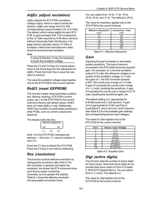
Chapter 8. MVS-<strong>STX</strong> Service Menu<br />
AdjEx (adjust excitation)<br />
AdjEx adjusts the <strong>STX</strong> PCB’s excitation<br />
voltage output, which is used to excite the<br />
sensors. AdjEx can range from 0 to 255,<br />
corresponding to approximately 5 to 12.9 Volts.<br />
The default, which varies slightly for each <strong>STX</strong><br />
PCB, is approximately 236. This corresponds<br />
to the 12 Volts required by K-M silicon sensors<br />
without Intrinsically Safe (IS) Barriers. Foil<br />
gage sensors typically require 10 Volts of<br />
excitation; refer to the manufacturer’s data<br />
sheet for recommended excitation.<br />
Note<br />
If using IS Barriers, it may be necessary<br />
to lower the excitation voltage.<br />
Press the F2 <strong>and</strong> F3 Keys for coarse adjustment<br />
or the Arrow Keys for fine adjustment of<br />
AdjEx. Press the Enter Key to save the new<br />
value in memory.<br />
The value for excitation voltage output applies<br />
only to the <strong>STX</strong> PCB for the current channel.<br />
RstE2 (reset EEPROM)<br />
This function resets most parameters (calibration,<br />
filtering, tracking, <strong>STX</strong> PCB’s current<br />
output, etc.) on the <strong>STX</strong> PCB for the current<br />
channel to factory-set default values. RstE2<br />
does not reset AdjEx or Iadj. Additionally,<br />
RstE2 has no effect on parameters residing on<br />
other PCBs, such as current outputs <strong>and</strong><br />
setpoints.<br />
The display looks like this:<br />
DEFAULT ADDR 12?<br />
Yes<br />
Addr 12 is the <strong>STX</strong> PCB’s hexadecimal<br />
address — first rack (‘1’), second position in<br />
rack (‘2’).<br />
Press the F1 Key to default the <strong>STX</strong> PCB.<br />
Press the F3 Key to exit without defaulting.<br />
Res (resolution)<br />
No<br />
F1 F2 F3<br />
This function controls effective resolution by<br />
changing the conversion rate of the 21-bit<br />
A/D converter. In general, the higher the<br />
resolution, the slower the <strong>STX</strong> conversion time<br />
(<strong>and</strong> time to switch monitoring<br />
channels), but the greater the stability.<br />
Table 8-1 shows the effective resolution<br />
<strong>and</strong> associated conversion times.<br />
You can select from 16 bt, 17 bt, 18 bt,<br />
19 bt, 20 bt, <strong>and</strong> 21 bt. The default is 20 bt.<br />
The value for resolution applies only to the<br />
<strong>STX</strong> PCB for the current channel.<br />
Effective Resolution Conversion Time<br />
(bits)<br />
(mS)<br />
16 25<br />
17 50<br />
18 83<br />
19 125<br />
20 250<br />
21 512<br />
Table 8-1. Effective Resolution<br />
Gain<br />
Adjusting the gain increases or decreases<br />
system sensitivity. The type of sensors<br />
connected to the <strong>STX</strong> determines the required<br />
gain. For example, for a nominal excitation<br />
output of 12 volts, the reference voltage is one<br />
quarter of the excitation voltage, or 3 volts.<br />
At a gain of 1, the A/D converter spreads<br />
2,097,152 counts over a range of ± 3 volts.<br />
A gain of 2 spreads the counts over a range<br />
of ± 1.5 volts, doubling the sensitivity. A gain<br />
of 4 spreads the counts over a range of ± 0.75<br />
volts, doubling the sensitivity again, etc.<br />
The default setting is 2, appropriate for<br />
K-M Microcell <strong>and</strong> L-Cell sensors. A gain<br />
of 4 is appropriate for K-M Load Disc II,<br />
Load St<strong>and</strong> II, <strong>and</strong> Load Link I <strong>and</strong> II sensors.<br />
See Table 8-2 for the available gain settings<br />
<strong>and</strong> corresponding sensor input voltages.<br />
The value for Gain applies only to the<br />
<strong>STX</strong> PCB for the current channel.<br />
Gain Sensor Input Voltage<br />
2 ±1.5<br />
1 ±3.0<br />
4 ±0.75<br />
8 ±0.375<br />
16 ±0.1875<br />
32 ±0.09375<br />
64 ±0.046875<br />
128 ±0.0234375<br />
Table 8-2. Amplifier Gain<br />
Digt (active digits)<br />
This function sets the number of active digits<br />
for input values. Note that active digits do not<br />
include fixed zeros (refer to Form in Chapter<br />
5, MVS-<strong>STX</strong> Display Menu). You can select<br />
from 4, 5, <strong>and</strong> 6. The default is 5.<br />
The value for Digt applies only to the<br />
<strong>STX</strong> PCB for the current channel.<br />
8-3