- Page 1 and 2:
Customer Interface Publication: KCH
- Page 3:
DescriptionMitsubishi microcomputer
- Page 7 and 8:
DescriptionMitsubishi microcomputer
- Page 9 and 10:
Pin DescriptionMitsubishi microcomp
- Page 11 and 12:
MemoryMitsubishi microcomputersM16C
- Page 13 and 14:
CPUMitsubishi microcomputersM16C /
- Page 15 and 16:
ResetMitsubishi microcomputersM16C
- Page 17 and 18:
ResetMitsubishi microcomputersM16C
- Page 19 and 20:
SFRMitsubishi microcomputersM16C /
- Page 21 and 22:
SFRMitsubishi microcomputersM16C /
- Page 23 and 24:
Memory Space Expansion FunctionsMit
- Page 25 and 26:
Memory Space Expansion FunctionsMit
- Page 27 and 28:
Memory Space Expansion FunctionsMit
- Page 29 and 30:
Processor ModeMitsubishi microcompu
- Page 31 and 32:
Processor ModeMitsubishi microcompu
- Page 33 and 34:
Bus SettingsMitsubishi microcompute
- Page 35 and 36:
Bus ControlMitsubishi microcomputer
- Page 37 and 38:
Bus ControlMitsubishi microcomputer
- Page 39 and 40:
Bus ControlMitsubishi microcomputer
- Page 41 and 42:
Clock Generating CircuitMitsubishi
- Page 43 and 44:
Clock Generating CircuitMitsubishi
- Page 45 and 46:
Clock Generating CircuitMitsubishi
- Page 47 and 48:
Status Transition Of BCLKMitsubishi
- Page 49 and 50:
Power controlMitsubishi microcomput
- Page 51 and 52:
InterruptMitsubishi microcomputersM
- Page 53 and 54:
InterruptMitsubishi microcomputersM
- Page 55 and 56:
InterruptMitsubishi microcomputersM
- Page 57 and 58:
InterruptMitsubishi microcomputersM
- Page 59 and 60:
InterruptMitsubishi microcomputersM
- Page 61 and 62:
InterruptMitsubishi microcomputersM
- Page 63 and 64:
InterruptMitsubishi microcomputersM
- Page 65 and 66:
InterruptMitsubishi microcomputersM
- Page 67 and 68:
________NMI InterruptMitsubishi mic
- Page 69 and 70:
Precautions for InterruptsMitsubish
- Page 71 and 72:
Watchdog TimerMitsubishi microcompu
- Page 73 and 74:
DMACMitsubishi microcomputersM16C /
- Page 75 and 76:
DMACMitsubishi microcomputersM16C /
- Page 77 and 78:
DMACMitsubishi microcomputersM16C /
- Page 79 and 80:
DMACMitsubishi microcomputersM16C /
- Page 81 and 82:
DMACMitsubishi microcomputersM16C /
- Page 83 and 84:
TimerMitsubishi microcomputersM16C
- Page 85 and 86:
Timer AMitsubishi microcomputersM16
- Page 87 and 88:
Timer AMitsubishi microcomputersM16
- Page 89 and 90:
Timer AMitsubishi microcomputersM16
- Page 91 and 92:
Timer AMitsubishi microcomputersM16
- Page 93 and 94:
Timer AMitsubishi microcomputersM16
- Page 95 and 96:
Timer BMitsubishi microcomputersM16
- Page 97 and 98:
Timer BMitsubishi microcomputersM16
- Page 99 and 100:
Timer BMitsubishi microcomputersM16
- Page 101 and 102:
Timers’ functions for three-phase
- Page 103 and 104:
Timers’ functions for three-phase
- Page 105 and 106:
Timers’ functions for three-phase
- Page 107 and 108:
Timers’ functions for three-phase
- Page 109 and 110:
Timers’ functions for three-phase
- Page 111 and 112:
Timers’ functions for three-phase
- Page 113 and 114:
Serial I/OMitsubishi microcomputers
- Page 115 and 116:
Serial I/OMitsubishi microcomputers
- Page 117 and 118:
Serial I/OMitsubishi microcomputers
- Page 119 and 120:
Serial I/OMitsubishi microcomputers
- Page 121 and 122:
Serial I/OMitsubishi microcomputers
- Page 123 and 124:
Clock synchronous serial I/O modeMi
- Page 125 and 126:
Clock synchronous serial I/O modeMi
- Page 127 and 128:
Clock synchronous serial I/O modeMi
- Page 129 and 130:
Clock asynchronous serial I/O (UART
- Page 131 and 132:
Clock asynchronous serial I/O (UART
- Page 133 and 134:
Clock asynchronous serial I/O (UART
- Page 135 and 136:
Clock asynchronous serial I/O (UART
- Page 137 and 138:
Clock asynchronous serial I/O (UART
- Page 139 and 140:
Clock asynchronous serial I/O (UART
- Page 141 and 142:
UART2 Special Mode RegisterMitsubis
- Page 143 and 144:
UART2 Special Mode RegisterMitsubis
- Page 145 and 146:
UART2 Special Mode Register 2Mitsub
- Page 147 and 148:
UART2 Special Mode Register 2Mitsub
- Page 149 and 150:
S I/O3, 4Mitsubishi microcomputersM
- Page 151 and 152:
S I/O3, 4Mitsubishi microcomputersM
- Page 153 and 154:
A-D ConverterMitsubishi microcomput
- Page 155 and 156:
A-D ConverterMitsubishi microcomput
- Page 157 and 158:
A-D ConverterMitsubishi microcomput
- Page 159 and 160:
A-D ConverterMitsubishi microcomput
- Page 161 and 162:
A-D ConverterMitsubishi microcomput
- Page 163 and 164:
D-A ConverterMitsubishi microcomput
- Page 165 and 166:
CRCMitsubishi microcomputersM16C /
- Page 167 and 168:
Programmable I/O PortMitsubishi mic
- Page 169 and 170:
Programmable I/O PortMitsubishi mic
- Page 171 and 172:
Programmable I/O PortMitsubishi mic
- Page 173 and 174:
Programmable I/O PortMitsubishi mic
- Page 175 and 176:
Programmable I/O PortMitsubishi mic
- Page 177 and 178:
Usage precautionMitsubishi microcom
- Page 179 and 180:
Usage precautionMitsubishi microcom
- Page 181 and 182:
Mitsubishi microcomputersM16C / 62
- Page 183 and 184:
Operating maximum frequency [MHZ]Op
- Page 185 and 186: Electrical characteristics (Vcc = 5
- Page 187 and 188: Timing (VCC=5V)Mitsubishi microcomp
- Page 189 and 190: Timing (VCC=5V)Mitsubishi microcomp
- Page 191 and 192: Timing (VCC=5V)Mitsubishi microcomp
- Page 193 and 194: Timing (Vcc = 5V)Mitsubishi microco
- Page 195 and 196: Timing (Vcc = 5V)Mitsubishi microco
- Page 197 and 198: Timing (Vcc = 5V)Mitsubishi microco
- Page 199 and 200: Electrical characteristics (Vcc = 3
- Page 201 and 202: Timing (Vcc = 3V)Mitsubishi microco
- Page 203 and 204: Timing (Vcc = 3V)Mitsubishi microco
- Page 205 and 206: Timing (Vcc = 3V)Mitsubishi microco
- Page 207 and 208: Timing (Vcc = 3V)Mitsubishi microco
- Page 209 and 210: Timing (Vcc = 3V)Mitsubishi microco
- Page 211 and 212: IssuancesignatureReceiptMitsubishi
- Page 213 and 214: Mitsubishi microcomputersM16C / 62
- Page 215 and 216: Mitsubishi microcomputersM16C / 62
- Page 217 and 218: IssuancesignatureReceiptMitsubishi
- Page 219 and 220: Mitsubishi microcomputersM16C / 62
- Page 221 and 222: Mitsubishi microcomputersM16C / 62
- Page 223 and 224: IssuancesignatureReceiptMitsubishi
- Page 225 and 226: Mitsubishi microcomputersM16C / 62
- Page 227 and 228: Mitsubishi microcomputersM16C / 62
- Page 229 and 230: IssuancesignatureReceiptMitsubishi
- Page 231 and 232: Mitsubishi microcomputersM16C / 62
- Page 233 and 234: Mitsubishi microcomputersM16C / 62
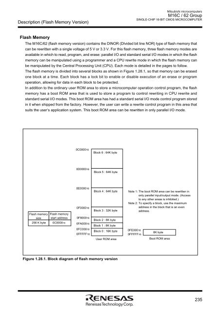
- Page 235: Operating maximum frequency [MHZ]De
- Page 239 and 240: CPU Rewrite Mode (Flash Memory Vers
- Page 241 and 242: CPU Rewrite Mode (Flash Memory Vers
- Page 243 and 244: CPU Rewrite Mode (Flash Memory Vers
- Page 245 and 246: CPU Rewrite Mode (Flash Memory Vers
- Page 247 and 248: CPU Rewrite Mode (Flash Memory Vers
- Page 249 and 250: CPU Rewrite Mode (Flash Memory Vers
- Page 251 and 252: Functions To Inhibit Rewriting (Fla
- Page 253 and 254: Appendix Standard Serial I/O Mode (
- Page 255 and 256: CNVSSRESETP93/DA0/TB3INP94/DA1/TB4I
- Page 257 and 258: Appendix Standard Serial I/O Mode (
- Page 259 and 260: Appendix Standard Serial I/O Mode (
- Page 261 and 262: Appendix Standard Serial I/O Mode (
- Page 263 and 264: Appendix Standard Serial I/O Mode (
- Page 265 and 266: Appendix Standard Serial I/O Mode (
- Page 267 and 268: Appendix Standard Serial I/O Mode (
- Page 269 and 270: Appendix Standard Serial I/O Mode (
- Page 271 and 272: Appendix Standard Serial I/O Mode (
- Page 273 and 274: 272Mitsubishi microcomputersM16C /
- Page 275 and 276: Mitsubishi microcomputersM16C / 62
- Page 277: MITSUBISHI SEMICONDUCTORSM16C/62 Gr