
You also want an ePaper? Increase the reach of your titles
YUMPU automatically turns print PDFs into web optimized ePapers that Google loves.
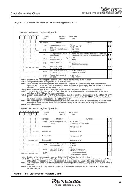
Clock Generating CircuitMitsubishi microcomputers<strong>M16C</strong> / <strong>62</strong> <strong>Group</strong>SINGLE-CHIP 16-BIT CMOS MICROCOMPUTERFigure 1.13.4 shows the system clock control registers 0 and 1.System clock control register 0 (Note 1)b7 b6 b5 b4 b3 b2 b1 b0Symbol Address When resetCM0 000616 4816Bit symbolCM00CM01CM02CM03CM04CM05CM06CM07Bit nameClock output functionselect bit(Valid only in single-chipmode)WAIT peripheral functionclock stop bitXCIN-XCOUT drive capacityselect bit (Note 2)Port XC select bitMain clock (XIN-XOUT)stop bit (Note 3, 4, 5)Main clock division selectbit 0 (Note 7)System clock select bit(Note 6)Functionb1 b00 0 : I/O port P570 1 : fC output1 0 : f8 output1 1 : f32 output0 : Do not stop peripheral function clock in wait mode1 : Stop peripheral function clock in wait mode (Note 8)0 : LOW1 : HIGH0 : I/O port1 : XCIN-XCOUT generation0 : On1 : Off0 : CM16 and CM17 valid1 : Division by 8 mode0 : XIN, XOUT1 : XCIN, XCOUTNote 1: Set bit 0 of the protect register (address 000A16) to “1” before writing to this register.Note 2: Changes to “1” when shiffing to stop mode and at a reset.Note 3: When entering power saving mode, main clock stops using this bit. When returning from stop mode andoperating with XIN, set this bit to “0”. When main clock oscillation is operating by itself, set system clock selectbit (CM07) to “1” before setting this bit to “1”.Note 4: When inputting external clock, only clock oscillation buffer is stopped and clock input is acceptable.Note 5: If this bit is set to “1”, XOUT turns “H”. The built-in feedback resistor remains being connected, so XIN turnspulled up to XOUT (“H”) via the feedback resistor.Note 6: Set port Xc select bit (CM04) to “1” and stabilize the sub-clock oscillating before setting to this bit from “0” to “1”.Do not write to both bits at the same time. And also, set the main clock stop bit (CM05) to “0” and stabilize themain clock oscillating before setting this bit from “1” to “0”.Note 7: This bit changes to “1” when shifting from high-speed/medium-speed mode to stop mode and at a reset. Whenshifting from low-speed/low power dissipation mode to stop mode, the value before stop mode is retained.Note 8: fC32 is not included.System clock control register 1 (Note 1)R W b7 b6 b5 b4 b3 b2 b1 b00 0 0 0Symbol Address When resetCM1 000716 2016Bit symbol Bit nameCM10 All clock stop control bit(Note4)CM15C<strong>M16C</strong>M17XIN-XOUT drive capacityselect bit (Note 2)Figure 1.13.4. Clock control registers 0 and 1Function0 : Clock on1 : All clocks off (stop mode)Reserved bit Always set to “0”Reserved bit Always set to “0”Reserved bit Always set to “0”Reserved bit Always set to “0”Main clock divisionselect bit 1 (Note 3)0 : LOW1 : HIGHb7 b60 0 : No division mode0 1 : Division by 2 mode1 0 : Division by 4 mode1 1 : Division by 16 modeNote 1: Set bit 0 of the protect register (address 000A16) to “1” before writing to this register.Note 2: This bit changes to “1” when shifting from high-speed/medium-speed mode to stop mode and at a reset. Whenshifting from low-speed/low power dissipation mode to stop mode, the value before stop mode is retained.Note 3: Can be selected when bit 6 of the system clock control register 0 (address 000616) is “0”. If “1”, division mode isfixed at 8.Note 4: If this bit is set to “1”, XOUT turns “H”, and the built-in feedback resistor is cut off. XCIN and XCOUT turn highimpedancestate.R W43