
You also want an ePaper? Increase the reach of your titles
YUMPU automatically turns print PDFs into web optimized ePapers that Google loves.
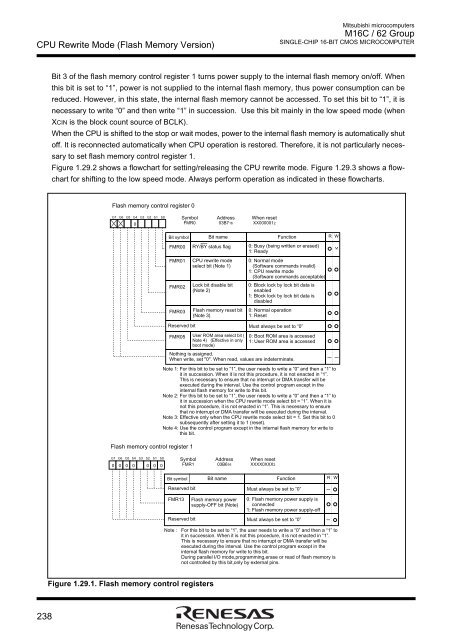
CPU Rewrite Mode (Flash Memory Version)Mitsubishi microcomputers<strong>M16C</strong> / <strong>62</strong> <strong>Group</strong>SINGLE-CHIP 16-BIT CMOS MICROCOMPUTERBit 3 of the flash memory control register 1 turns power supply to the internal flash memory on/off. Whenthis bit is set to “1”, power is not supplied to the internal flash memory, thus power consumption can bereduced. However, in this state, the internal flash memory cannot be accessed. To set this bit to “1”, it isnecessary to write “0” and then write “1” in succession. Use this bit mainly in the low speed mode (whenXCIN is the block count source of BCLK).When the CPU is shifted to the stop or wait modes, power to the internal flash memory is automatically shutoff. It is reconnected automatically when CPU operation is restored. Therefore, it is not particularly necessaryto set flash memory control register 1.Figure 1.29.2 shows a flowchart for setting/releasing the CPU rewrite mode. Figure 1.29.3 shows a flowchartfor shifting to the low speed mode. Always perform operation as indicated in these flowcharts.Flash memory control register 0b7 b6 b5 b4 b3 b2 b1 b00Symbol Address When resetFMR0 03B716 XX0000012Bit symbol Bit name Function R WFMR00 RY/BY status flag 0: Busy (being written or erased) 1: ReadyFMR01FMR02FMR03FMR05Flash memory control register 1CPU rewrite modeselect bit (Note 1)Lock bit disable bit(Note 2)Flash memory reset bit(Note 3)User ROM area select bit (Note 4) (Effective in onlyboot mode)0: Normal mode(Software commands invalid)1: CPU rewrite mode(Software commands acceptable)0: Block lock by lock bit data isenabled1: Block lock by lock bit data isdisabled0: Normal operation1: ResetReserved bit Must always be set to “0”0: Boot ROM area is accessed1: User ROM area is accessedNothing is assigned.When write, set "0". When read, values are indeterminate. Note 1: For this bit to be set to “1”, the user needs to write a “0” and then a “1” toit in succession. When it is not this procedure, it is not enacted in “1”.This is necessary to ensure that no interrupt or DMA transfer will beexecuted during the interval. Use the control program except in theinternal flash memory for write to this bit.Note 2: For this bit to be set to “1”, the user needs to write a “0” and then a “1” toit in succession when the CPU rewrite mode select bit = “1”. When it isnot this procedure, it is not enacted in “1”. This is necessary to ensurethat no interrupt or DMA transfer will be executed during the interval.Note 3: Effective only when the CPU rewrite mode select bit = 1. Set this bit to 0subsequently after setting it to 1 (reset).Note 4: Use the control program except in the internal flash memory for write tothis bit.b7 b6 b5 b4 b3 b2 b1 b00 0 0 0 0 0 0Symbol Address When resetFMR1 03B616 XXXX0XXX2Bit symbol Bit name Function R WReserved bit Must always be set to “0”FMR13Flash memory powersupply-OFF bit (Note)0: Flash memory power supply isconnected1: Flash memory power supply-offReserved bit Must always be set to “0”Note : For this bit to be set to “1”, the user needs to write a “0” and then a “1” toit in succession. When it is not this procedure, it is not enacted in “1”.This is necessary to ensure that no interrupt or DMA transfer will beexecuted during the interval. Use the control program except in theinternal flash memory for write to this bit.During parallel I/O mode,programming,erase or read of flash memory isnot controlled by this bit,only by external pins.Figure 1.29.1. Flash memory control registers238