

Online proceedings - EDA Publishing Association
Online proceedings - EDA Publishing Association
Online proceedings - EDA Publishing Association
- No tags were found...

You also want an ePaper? Increase the reach of your titles
YUMPU automatically turns print PDFs into web optimized ePapers that Google loves.
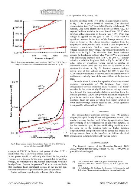
Drain source leakage current (A)Reverse current (A)2.5E-032.0E-031.5E-031.0E-035.0E-040.0E+00250 o C200 o C0 500 1000 1500 2000Reverse voltage (V)Fig. 6. Reverse current-voltage characteristics at 200 o C and 250 o C for thesample No.2 of controlled-avalanche diode (also used in Fig. 5)2.E-041.E-040.E+00200 o C,Vgs=0150 o C,Vgs=2.0V150 o C, Vgs=0175 o C, Vgs=00 500 1000 1500Drain source voltage (V)24-26 September 2008, Rome, Italydielectric interface on the level of the leakage current is shownin Fig. 7 for a power MOSFET transistor. The electricalcharacteristics from Fig.7 are exhibited by the cellular drain PNjunction. Like in the planar silicon diode case from Fig.2, theslope of the linear variation increases from 150 to 200 o C whenzero bias voltage is applied on the gate (Vgs = 0V). When biasvoltage is applied on the gate at 150 o C (Vgs =2.0 V)significant increase in the level of the leakage current takesplace on behalf of the silicon–dielectric interface from theperiphery of drain junction cells. In such a case the portion ofelectrical characteristic fitted to linear variation is morereduced than at zero bias voltage. The behavior is similar to thediode case in Fig.5. The deviation from linear variationtowards the breakdown voltage when Vgs = 0 V is accentuatedwith temperature increase from 150 o C to 200 o C. Similarbehavior is valid for the planar diode in Fig.2a. At 200 o C theinitial value of breakdown voltage cannot be reached atreasonable current level and this behavior is similar to thesituation for diodes in Fig. 2b. Practical constant leakagecurrent level at low voltage in Fig.7 for 150 o C and Vgs=2.0Vcannot be attributed to the bulk diffusion current becausein this case, evidently most of the current flows at the junctionedge.From the above it results that a portion of the experimentalelectrical characteristic of PN junctions from powersemiconductor devices manifests linear variation. This linearvariation is the result of significant reverse leakage currentflow through the semiconductor-dielectric interface from thejunction periphery. Above the specified maximum temperaturegiven in the device data sheets, the leakage current in theinterfacial layer can cause deviation from linear variation atlower applied voltage than the specified one. Device operationis not possible without risk of failure.IV. CONCLUSIONSThe semiconductor-dielectric interface from PN junctionperiphery is a path for significant leakage reverse current. Thisinterface is a very thin layer with different properties than thosecorresponding to the semiconductor or dielectric material. Inthis thin interfacial layer, the junction blocking capability is notthe same as in the junction bulk. At higher junctiontemperature than the specified one in the device data sheets, theleakage current flow at the interface can initiate electricalcharacteristic instability followed by device failure.Fig.7. Drain leakage current characteristics from 150 o C to 200 o C for apower MOS transistor (4A, 1000 V)example at 250 o C in Fig.6 a peak power of about 2 W isreached for 1000 V sine wave applied voltage.If this power would be uniformly distributed in the junctionvolume, as it is the case for the power generated at forward biasvoltage, its contribution to the junction temperature would notbe significant. Because the power of 2 W is concentrated in thethin interfacial layer, significant increase in the junction nonuniformtemperature is possible at the junction periphery.Further evidence regarding the influence of the siliconACKNOWLEDGMENTThe financial support of the Romanian National R&DCEEX Program for this work, contract No. 310 /13.09.2006, isgratefully acknowledged.REFERENCES[1] R.R. Verdeber et al, “SiO 2/Si 3N 4 passivation of high powerrectifiers”, IEEE Trans. Electron Devices, Vol. ED-17, pp.797-800,1970.[2] S. Salkalachen, N. Krishnan, S. Krishnan, H. Satyamurthy andK.Srinivas, “Edge passivation and related electrical stability in.©<strong>EDA</strong> <strong>Publishing</strong>/THERMINIC 2008 146ISBN: 978-2-35500-008-9


