

Online proceedings - EDA Publishing Association
Online proceedings - EDA Publishing Association
Online proceedings - EDA Publishing Association
- No tags were found...

You also want an ePaper? Increase the reach of your titles
YUMPU automatically turns print PDFs into web optimized ePapers that Google loves.
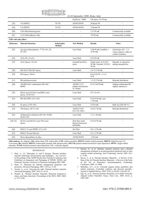
24-26 September 2008, Rome, ItalyFlashLine3000) CB-epoxy: 0.6 W/mk[53] VA-MWNT TCVD ASTM D5470 28 Kmm 2 /W -[54] VA-MWNT TCVD ASTM D5470 15 Kmm 2 /W -[90] CNF-filled thermal grease - - 1.25 W/mK Commercially available[91] A-CF-filled adhesive film - - 750 W/mk Commercially availableTIMs with other fillersReference Material Structure FabricationMethodTest Method Results Notes[55] Ag-epoxy/thermoplastic, 77-93 wt%, 28-62 vol%- Laser flash 3-60 W/mK, bondline 1-10 W/mKAnisotropy of k: ~1.5,3 layer analysis: effect ofcontact resistance[56] Al 2O 3-PS, 10 wt% - Laser flash 0.18 W/mK -[57] Al 2O 3-Epoxy, 50 wt% - Guarded heat flowmeterSingle mode: 0.35-0.65W/mK, bimodal: 0.38-0.4W/mkBimodal. k reduced byadding nanoparticles[58] BN/Al 2O 3/TiB 2/SiC-epoxy - Laser flash 3.9-13.5 W/mK -[59] BN-Epoxy, 30wt% - 0.6-0.9 K/W, 1.2-1.6K/W-[11] BN-polybenzoxazine - Laser flash 1.5-32.5 W/mK Bimodal distribution[60] AlN/BN/AlN+wollastonite/AlN+SiC-HDPE- ASTM C1113(Mathis InstrumentsTC Probe)0.75-3.66 W/mK Adding wollastonite/SiCslightly enhances k[35] SiO 2(3 µm)/Al 2O 3(0.3 µm)/BN(1 µm)-Epoxy, 10-60 wt%- Laser flash 0.5-1.0 wt% -[61] BN/AlN-PBT, 0-25 vol% - Laser flash 0.4-0.8 W/mK, max1.1W/mK-[62] Ni-epoxy, 0-30 vol% - Laser flash 2.0 W/mK High Tg (220-250 °C)[12] AlN-Epoxy, 60-74 vol% - ASTM E1530(ULVAC GH1)4.0-8.2 W/mK Bimodal distribution[63] AlN(particles/whiskers)/AlN+SiC-PVDF,40-60 vol%- Laser flash 1.3-11 W/mK -[64, 65] SiC(0.2 µm)/SiC(0.2 µm)+Ni(5 µm)-Epoxy- Heat flow meter(Kyoto ElectronicsQTM500)0.5-0.6 W/mK -[66] BN(0.5-15 µm)-HDPE, 0-35 vol% - Hot Disk 0.8-1.2 W/mK -[67] BN(0.3-20 µm)-Silicone - Laser flash 0.5-1.2 W/mK -[92] Micro-&nanofibers-In alloy - ASTM D5470 ~8 W/mK -Abbreviations: A-: aligned-, CB: carbon black, CF: carbon fiber, CNF: carbon nanofiber, DWNT: double-walled nanotube, HiPCO: High-Pressure COConversion, IR: infrared, MWNT: multiwalled nanotube, PA: photoacoustic, PECVD: plasma-enhanced chemical vapor deposition, SWNT: single-wallednanotube, TCVD: thermal chemical vapor deposition, VA-: vertically aligned-REFERENCES1. Dani, A., J.C. Matayabas Jr, and P. Koning. Thermal interfacematerial technology advancements and challenges - An overview.in Proceedings of the ASME/Pacific Rim Technical Conference andExhibition on Integration and Packaging of MEMS, NEMS, andElectronic Systems: Advances in Electronic Packaging 2005. 2005.2. Dean, N., Materials for thermal management properties andprocesses. Advanced Packaging, 2003. 12(3): p. 15-20.3. Gowda, A., et al., Choosing the right: Thermal interface material.Advanced Packaging, 2005. 14(3): p. 14-18.4. Prasher, R., Thermal interface materials: Historical perspective,status, and future directions. Proceedings of the IEEE, 2006. 94(8):p. 1571-1586.5. Samson, E., et al., Interface material selection and a thermalmanagement technique in second-generation platforms built on intelcentrino mobile technology. Intel Technology Journal, 2005. 9(1):p. 75-86.6. Sarvar, F., et al. Thermal Interface Materials - A Review of theState of the Art Thermal Interface Materials - A Review of the Stateof the Art. in Electronics Systemintegration TechnologyConference, 2006. 1st. 2006.7. Melechko, A.V., et al., Vertically aligned carbon nanofibers andrelated structures: Controlled synthesis and directed assembly.Journal of Applied Physics, 2005. 97(4): p. 041301-1-041301-39.8. Ngo, Q., et al., Thermal Interface Properties of Cu-filled VerticallyAligned Carbon Nanofiber Arrays. Nano Lett., 2004. 4(12): p.2403-2407.©<strong>EDA</strong> <strong>Publishing</strong>/THERMINIC 2008 160ISBN: 978-2-35500-008-9


