

Online proceedings - EDA Publishing Association
Online proceedings - EDA Publishing Association
Online proceedings - EDA Publishing Association
- No tags were found...

You also want an ePaper? Increase the reach of your titles
YUMPU automatically turns print PDFs into web optimized ePapers that Google loves.
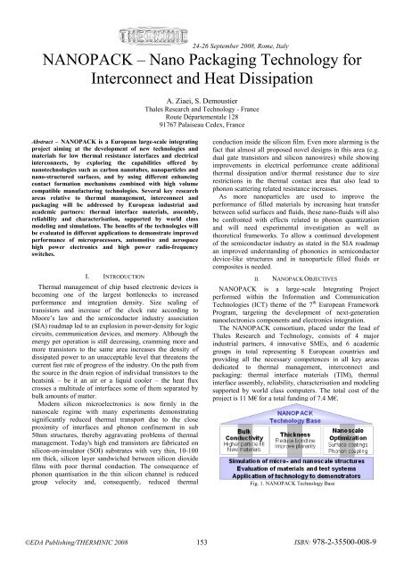
24-26 September 2008, Rome, ItalyNANOPACK – Nano Packaging Technology forInterconnect and Heat DissipationA. Ziaei, S. DemoustierThales Research and Technology - FranceRoute Départementale 12891767 Palaiseau Cedex, FranceAbstract – NANOPACK is a European large-scale integratingproject aiming at the development of new technologies andmaterials for low thermal resistance interfaces and electricalinterconnects, by exploring the capabilities offered bynanotechnologies such as carbon nanotubes, nanoparticles andnano-structured surfaces, and by using different enhancingcontact formation mechanisms combined with high volumecompatible manufacturing technologies. Several key researchareas relative to thermal management, interconnect andpackaging will be addressed by European industrial andacademic partners: thermal interface materials, assembly,reliability and characterisation, supported by world classmodeling and simulations. The benefits of the technologies willbe evaluated in different applications to demonstrate improvedperformance of microprocessors, automotive and aerospacehigh power electronics and high power radio-frequencyswitches.I. INTRODUCTIONThermal management of chip based electronic devices isbecoming one of the largest bottlenecks to increasedperformance and integration density. Size scaling oftransistors and increase of the clock rate according toMoore’s law and the semiconductor industry association(SIA) roadmap led to an explosion in power-density for logiccircuits, communication devices, and memory. Although theenergy per operation is still decreasing, cramming more andmore transistors to the same area increases the density ofdissipated power to an unacceptable level that threatens thecurrent fast rate of progress of the industry. On the path fromthe source in the drain region of individual transistors to theheatsink – be it an air or a liquid cooler – the heat fluxcrosses a multitude of interfaces some of them separated bybulk amounts of matter.Modern silicon microelectronics is now firmly in thenanoscale regime with many experiments demonstratingsignificantly reduced thermal transport due to the closeproximity of interfaces and phonon confinement in sub50nm structures, thereby aggravating problems of thermalmanagement. Today's high end transistors are fabricated onsilicon-on-insulator (SOI) substrates with very thin, 10-100nm thick, silicon layer sandwiched between silicon dioxidefilms with poor thermal conduction. The consequence ofphonon quantisation in the thin silicon channel is reducedgroup velocity and, consequently, reduced thermalconduction inside the silicon film. Even more alarming is thefact that almost all proposed novel designs in this area (e.g.dual gate transistors and silicon nanowires) while showingimprovements in electrical performance create additionalthermal dissipation and/or thermal resistance due to sizerestrictions in the thermal contact area that also lead tophonon scattering related resistance increases.As more nanoparticles are used to improve theperformance of filled materials by increasing heat transferbetween solid surfaces and fluids, these nano-fluids will alsobe confronted with effects related to phonon quantizationand will need experimental investigation as well astheoretical frameworks. To allow a continued developmentof the semiconductor industry as stated in the SIA roadmapan improved understanding of phononics in semiconductordevice-like structures and in nanoparticle filled fluids orcomposites is needed.II. NANOPACK OBJECTIVESNANOPACK is a large-scale Integrating Projectperformed within the Information and CommunicationTechnologies (ICT) theme of the 7 th European FrameworkProgram, targeting the development of next-generationnanoelectronics components and electronics integration.The NANOPACK consortium, placed under the lead ofThales Research and Technology, consists of 4 majorindustrial partners, 4 innovative SMEs, and 6 academicgroups in total representing 8 European countries andproviding all the necessary competences in all key areasdedicated to thermal management, interconnect andpackaging: thermal interface materials (TIM), thermalinterface assembly, reliability, characterisation and modelingsupported by world class computers. The total cost of theproject is 11 M€ for a total funding of 7.4 M€.Fig. 1. NANOPACK Technology Base©<strong>EDA</strong> <strong>Publishing</strong>/THERMINIC 2008 153ISBN: 978-2-35500-008-9


