- Page 2:
Thixoforming Semi-solid Metal Proce
- Page 5 and 6:
Further Reading Herlach, D. M. (ed.
- Page 7 and 8:
The Editors Prof. Dr. G. Hirt Insti
- Page 9 and 10:
VI Contents 1.3.5.2 Other Aluminium
- Page 11 and 12:
VIII Contents 4.6.1 Thixocasting 13
- Page 13 and 14:
X Contents 7.4.2 Isothermal Non-ste
- Page 15 and 16:
XII Contents 9.4.1.3 Simulation Res
- Page 18:
Preface Semi-solid forming of metal
- Page 21 and 22:
XVIII List of Contributors Andreas
- Page 23 and 24:
XX List of Contributors Alexander S
- Page 25 and 26:
2j 1 Semi-solid Forming of Aluminiu
- Page 27 and 28:
4j 1 Semi-solid Forming of Aluminiu
- Page 29 and 30:
6j 1 Semi-solid Forming of Aluminiu
- Page 31 and 32:
8j 1 Semi-solid Forming of Aluminiu
- Page 33 and 34:
10j 1 Semi-solid Forming of Alumini
- Page 35 and 36:
12j 1 Semi-solid Forming of Alumini
- Page 37 and 38:
14j 1 Semi-solid Forming of Alumini
- Page 39 and 40:
16j 1 Semi-solid Forming of Alumini
- Page 41 and 42:
18j 1 Semi-solid Forming of Alumini
- Page 43 and 44:
20j 1 Semi-solid Forming of Alumini
- Page 45 and 46:
Table 1.1 Overview of semi-solid pr
- Page 47 and 48:
24j 1 Semi-solid Forming of Alumini
- Page 49 and 50:
26j 1 Semi-solid Forming of Alumini
- Page 52:
Part One Material Fundamentals of M
- Page 55 and 56:
32j 2 Metallurgical Aspects of SSM
- Page 57 and 58:
34j 2 Metallurgical Aspects of SSM
- Page 59 and 60:
36j 2 Metallurgical Aspects of SSM
- Page 61 and 62:
38j 2 Metallurgical Aspects of SSM
- Page 63 and 64:
40j 2 Metallurgical Aspects of SSM
- Page 65 and 66:
42j 2 Metallurgical Aspects of SSM
- Page 67 and 68:
44j 3 Material Aspects of Steel Thi
- Page 69 and 70:
46j 3 Material Aspects of Steel Thi
- Page 71 and 72:
48j 3 Material Aspects of Steel Thi
- Page 73 and 74:
50j 3 Material Aspects of Steel Thi
- Page 75 and 76:
52j 3 Material Aspects of Steel Thi
- Page 77 and 78:
54j 3 Material Aspects of Steel Thi
- Page 79 and 80:
56j 3 Material Aspects of Steel Thi
- Page 81 and 82:
58j 3 Material Aspects of Steel Thi
- Page 83 and 84:
60j 3 Material Aspects of Steel Thi
- Page 85 and 86:
62j 3 Material Aspects of Steel Thi
- Page 87 and 88:
64j 3 Material Aspects of Steel Thi
- Page 89 and 90:
66j 3 Material Aspects of Steel Thi
- Page 91 and 92:
68j 3 Material Aspects of Steel Thi
- Page 93 and 94:
70j 3 Material Aspects of Steel Thi
- Page 95 and 96:
72j 3 Material Aspects of Steel Thi
- Page 97 and 98:
74j 3 Material Aspects of Steel Thi
- Page 99 and 100:
76j 3 Material Aspects of Steel Thi
- Page 101 and 102:
78j 3 Material Aspects of Steel Thi
- Page 103 and 104:
80j 3 Material Aspects of Steel Thi
- Page 105 and 106:
82j 3 Material Aspects of Steel Thi
- Page 107 and 108:
84j 3 Material Aspects of Steel Thi
- Page 109 and 110:
86j 3 Material Aspects of Steel Thi
- Page 111 and 112:
88j 3 Material Aspects of Steel Thi
- Page 113 and 114:
Temperature (ºC) 1550 1500 1450 14
- Page 115 and 116:
92j 3 Material Aspects of Steel Thi
- Page 117 and 118:
94j 3 Material Aspects of Steel Thi
- Page 119 and 120:
96j 3 Material Aspects of Steel Thi
- Page 121 and 122:
98j 3 Material Aspects of Steel Thi
- Page 123 and 124:
100j 3 Material Aspects of Steel Th
- Page 125 and 126:
102j 3 Material Aspects of Steel Th
- Page 127 and 128:
104j 3 Material Aspects of Steel Th
- Page 129 and 130:
106j 4 Design of Al and Al-Li Alloy
- Page 131 and 132:
108j 4 Design of Al and Al-Li Alloy
- Page 133 and 134:
110j 4 Design of Al and Al-Li Alloy
- Page 135 and 136:
112j 4 Design of Al and Al-Li Alloy
- Page 137 and 138:
114j 4 Design of Al and Al-Li Alloy
- Page 139 and 140:
116j 4 Design of Al and Al-Li Alloy
- Page 141 and 142:
118j 4 Design of Al and Al-Li Alloy
- Page 143 and 144:
120j 4 Design of Al and Al-Li Alloy
- Page 145 and 146:
122j 4 Design of Al and Al-Li Alloy
- Page 147 and 148:
124j 4 Design of Al and Al-Li Alloy
- Page 149 and 150:
126j 4 Design of Al and Al-Li Alloy
- Page 151 and 152:
128j 4 Design of Al and Al-Li Alloy
- Page 153 and 154:
130j 4 Design of Al and Al-Li Alloy
- Page 155 and 156:
132j 4 Design of Al and Al-Li Alloy
- Page 157 and 158:
134j 4 Design of Al and Al-Li Alloy
- Page 159 and 160:
136j 4 Design of Al and Al-Li Alloy
- Page 161 and 162:
138j 4 Design of Al and Al-Li Alloy
- Page 163 and 164:
140j 4 Design of Al and Al-Li Alloy
- Page 165 and 166:
142j 4 Design of Al and Al-Li Alloy
- Page 167 and 168:
144j 4 Design of Al and Al-Li Alloy
- Page 170 and 171:
5 Thermochemical Simulation of Phas
- Page 172 and 173:
here it can be assumed that the dat
- Page 174 and 175:
Figure 5.2 Calculated temperature v
- Page 176 and 177:
Figure 5.4 Composition profiles of
- Page 178 and 179:
It is clear that C has by far the s
- Page 180 and 181:
Figure 5.7 The density of X210CrW12
- Page 182 and 183:
5.3 Calculations for the Bearing St
- Page 184 and 185:
Figure 5.11 Composition profiles of
- Page 186 and 187:
Figure 5.14 The density of 100Cr6.
- Page 188 and 189:
area which is available for heat tr
- Page 190:
Part Two Modelling the Flow Behavio
- Page 193 and 194:
170j 6 Modelling the Flow Behaviour
- Page 195 and 196:
172j 6 Modelling the Flow Behaviour
- Page 197 and 198:
174j 6 Modelling the Flow Behaviour
- Page 199 and 200:
176j 6 Modelling the Flow Behaviour
- Page 201 and 202:
178j 6 Modelling the Flow Behaviour
- Page 203 and 204:
180j 6 Modelling the Flow Behaviour
- Page 205 and 206:
182j 6 Modelling the Flow Behaviour
- Page 207 and 208:
184j 6 Modelling the Flow Behaviour
- Page 209 and 210:
186j 6 Modelling the Flow Behaviour
- Page 211 and 212:
188j 6 Modelling the Flow Behaviour
- Page 213 and 214:
190j 6 Modelling the Flow Behaviour
- Page 215 and 216:
192j 6 Modelling the Flow Behaviour
- Page 217 and 218:
194j 6 Modelling the Flow Behaviour
- Page 219 and 220:
196j 6 Modelling the Flow Behaviour
- Page 221 and 222:
198j 6 Modelling the Flow Behaviour
- Page 223 and 224:
200j 6 Modelling the Flow Behaviour
- Page 225 and 226:
202j 6 Modelling the Flow Behaviour
- Page 227 and 228:
204j 6 Modelling the Flow Behaviour
- Page 229 and 230:
206j 6 Modelling the Flow Behaviour
- Page 231 and 232:
208j 6 Modelling the Flow Behaviour
- Page 233 and 234:
210j 6 Modelling the Flow Behaviour
- Page 235 and 236:
212j 6 Modelling the Flow Behaviour
- Page 237 and 238:
214j 6 Modelling the Flow Behaviour
- Page 239 and 240:
216j 6 Modelling the Flow Behaviour
- Page 241 and 242: 218j 6 Modelling the Flow Behaviour
- Page 244 and 245: 7 A Physical and Micromechanical Mo
- Page 246 and 247: 3. Macroscopic averages or homogeni
- Page 248 and 249: displacement boundary conditions or
- Page 250 and 251: and liquid are both assumed to be i
- Page 252 and 253: are the strain rate concentration t
- Page 254 and 255: Semi-solid viscosity (Pa s) into cl
- Page 256 and 257: Load (kN) strain to rupture, leadin
- Page 258 and 259: Load (kN) 7 6 5 4 3 2 1 0 0 7.5 Con
- Page 260 and 261: adius R radius of the spherical inc
- Page 262: Part Three Tool Technologies for Fo
- Page 265 and 266: 242j 8 Tool Technologies for Formin
- Page 267 and 268: 244j 8 Tool Technologies for Formin
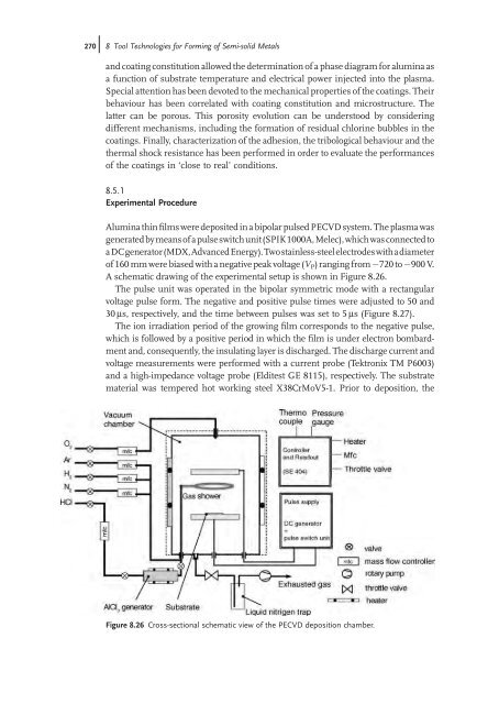
- Page 269 and 270: 246j 8 Tool Technologies for Formin
- Page 271 and 272: 248j 8 Tool Technologies for Formin
- Page 273 and 274: 250j 8 Tool Technologies for Formin
- Page 275 and 276: 252j 8 Tool Technologies for Formin
- Page 277 and 278: 254j 8 Tool Technologies for Formin
- Page 279 and 280: 256j 8 Tool Technologies for Formin
- Page 281 and 282: 258j 8 Tool Technologies for Formin
- Page 283 and 284: 260j 8 Tool Technologies for Formin
- Page 285 and 286: 262j 8 Tool Technologies for Formin
- Page 287 and 288: 264j 8 Tool Technologies for Formin
- Page 289 and 290: 266j 8 Tool Technologies for Formin
- Page 291: 268j 8 Tool Technologies for Formin
- Page 295 and 296: 272j 8 Tool Technologies for Formin
- Page 297 and 298: 274j 8 Tool Technologies for Formin
- Page 299 and 300: 276j 8 Tool Technologies for Formin
- Page 301 and 302: 278j 8 Tool Technologies for Formin
- Page 303 and 304: 280j 8 Tool Technologies for Formin
- Page 305 and 306: 282j 8 Tool Technologies for Formin
- Page 307 and 308: 284j 8 Tool Technologies for Formin
- Page 309 and 310: 286j 8 Tool Technologies for Formin
- Page 311 and 312: 288j 8 Tool Technologies for Formin
- Page 313 and 314: 290j 8 Tool Technologies for Formin
- Page 315 and 316: 292j 8 Tool Technologies for Formin
- Page 317 and 318: 294j 8 Tool Technologies for Formin
- Page 319 and 320: 296j 8 Tool Technologies for Formin
- Page 321 and 322: 298j 8 Tool Technologies for Formin
- Page 323 and 324: 300j 8 Tool Technologies for Formin
- Page 325 and 326: 302j 8 Tool Technologies for Formin
- Page 327 and 328: 304j 8 Tool Technologies for Formin
- Page 329 and 330: 306j 8 Tool Technologies for Formin
- Page 331 and 332: 308j 8 Tool Technologies for Formin
- Page 334 and 335: 9 Rheocasting of Aluminium Alloys a
- Page 336 and 337: Figure 9.2 Processes for the semi-s
- Page 338 and 339: Two Italian companies gained the fi
- Page 340 and 341: 9.2 SSM Casting Processesj317 For t
- Page 342 and 343:
Figure 9.7 Oil pump cover for Honda
- Page 344 and 345:
Figure 9.9 Middle temperature cours
- Page 346 and 347:
Figure 9.12 Components of cartridge
- Page 348 and 349:
Figure 9.15 Process adapted multipa
- Page 350 and 351:
step-shot experiments. It is also s
- Page 352 and 353:
Figure 9.18 (a) Meander tool for fl
- Page 354 and 355:
Figure 9.19 (a, b) Wear appears in
- Page 356 and 357:
Table 9.2 Temperature determination
- Page 358 and 359:
and are plausible on the left. Furt
- Page 360 and 361:
Figure 9.27 Development of the micr
- Page 362 and 363:
some places can be observed as smal
- Page 364 and 365:
Figure 9.31 Simulation of the metal
- Page 366 and 367:
Figure 9.33 So-called Constant Temp
- Page 368 and 369:
Figure 9.35 Comparison of the micro
- Page 370 and 371:
9.4 Rheoroutej347 If rounding of th
- Page 372 and 373:
9.4.1.2 Parameters: Cooling to the
- Page 374 and 375:
Figure 9.36 Results of the 2D-MICRE
- Page 376 and 377:
homogeneous microstructure and no d
- Page 378 and 379:
grain fragment density [mm -1 ] 200
- Page 380 and 381:
can be considered for rheocasting o
- Page 382 and 383:
Figure 9.44 Microstructure of Zr/Sc
- Page 384 and 385:
Figure 9.45 MAGMAsoft simulation: c
- Page 386 and 387:
The cooling to the process temperat
- Page 388 and 389:
D grain diameter of a circle DGM De
- Page 390 and 391:
27 Doppelbauer, M. (2003) Wirtschaf
- Page 392 and 393:
10 Thixoforging and Rheoforging of
- Page 394 and 395:
1970s [7]. Also, the quality of the
- Page 396 and 397:
10.3 Heating and Forming Operations
- Page 398 and 399:
With the solution of the Equations
- Page 400 and 401:
10.3.1.2 Modelling of Inductive Hea
- Page 402 and 403:
material properties have to be cons
- Page 404 and 405:
10.3 Heating and Forming Operations
- Page 406 and 407:
Figure 10.9 Experimental results, d
- Page 408 and 409:
Figure 10.12 Segregation in compone
- Page 410 and 411:
10.3.4 Thixoforging of Steel In thi
- Page 412 and 413:
10.3.5 Thixojoining of Steel In the
- Page 414 and 415:
einforcing element. The possibiliti
- Page 416 and 417:
Figure 10.20 The robot controller a
- Page 418 and 419:
Figure 10.21 Experimental results w
- Page 420 and 421:
Figure 10.24 Design and working pri
- Page 422 and 423:
The investigations show that the rh
- Page 424 and 425:
Figure 10.31 Scheme of the heat tra
- Page 426 and 427:
Table 10.2 Definition of boundary c
- Page 428 and 429:
Figure 10.35 Experimental and simul
- Page 430 and 431:
References 1 Koesling, D., Tinius,
- Page 432:
steel billets into the semi-solid s
- Page 435 and 436:
412j 11 Thixoextrusion The followin
- Page 437 and 438:
414j 11 Thixoextrusion channel with
- Page 439 and 440:
416j 11 Thixoextrusion parameter co
- Page 441 and 442:
418j 11 Thixoextrusion Both concept
- Page 443 and 444:
420j 11 Thixoextrusion should be ju
- Page 445 and 446:
422j 11 Thixoextrusion Figure 11.8
- Page 447 and 448:
424j 11 Thixoextrusion Table 11.4 C
- Page 449 and 450:
426j 11 Thixoextrusion Temperature
- Page 451 and 452:
428j 11 Thixoextrusion impacts. Ext
- Page 453 and 454:
430j 11 Thixoextrusion Figure 11.17
- Page 455 and 456:
432j 11 Thixoextrusion shell format
- Page 457 and 458:
434j 11 Thixoextrusion Figure 11.24
- Page 459 and 460:
436j 11 Thixoextrusion Table 11.6 P
- Page 461 and 462:
438j 11 Thixoextrusion Figure 11.30
- Page 463 and 464:
440j 11 Thixoextrusion solidificati
- Page 465 and 466:
442j 11 Thixoextrusion GPa pressure
- Page 467 and 468:
444j Index arbitrary volume element
- Page 469 and 470:
446j Index equilibrium tests 141 eq
- Page 471 and 472:
448j Index - importance 273 ion flu
- Page 473 and 474:
450j Index oxygen-sensitive element
- Page 475 and 476:
452j Index - thixoforming 241 semi-
- Page 477:
454j Index - high pressure 131 - sc