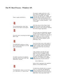
Tweaking Optimizing Windows.pdf - GEGeek
Tweaking Optimizing Windows.pdf - GEGeek
Tweaking Optimizing Windows.pdf - GEGeek

Create successful ePaper yourself
Turn your PDF publications into a flip-book with our unique Google optimized e-Paper software.
efreshing can be delayed for as long as possible. This reduces the number of refreshes and increases the effective memory<br />
bandwidth.<br />
An alternative method would be to greatly increase the value of the Refresh Interval or Refresh Mode Select feature to boost<br />
bandwidth and use this feature to maintain the data integrity of the memory cells. As ultra long refresh intervals (i.e. 64 or 128<br />
µsec) can cause memory cells to lose their contents, setting a low SDRAM Idle Limit like 0 or 8 cycles allows the memory cells to be<br />
refreshed more often, with a high chance of those refreshes being done during idle cycles. This appears to combine the best of both<br />
worlds - a long bank active period when the memory controller is being stressed and more refreshes when the memory controller is<br />
idle.<br />
In reality though, this is a really unreliable way of ensuring sufficient refresh cycles since it depends on the vagaries of memory<br />
usage to provide sufficient idle cycles to trigger the refreshes. If your memory subsystem is constantly in heavy use, there may not<br />
be any idle cycles to trigger an early refresh. This will cause the memory cells to lose their contents because they are not being<br />
refreshed enough. Therefore, it is recommended that you maintain a proper refresh interval and disable this feature. This will<br />
allow you to boost memory bandwidth by delaying refreshes for as long as possible and still maintain the data integrity of the<br />
memory cells via regular and reliable refresh cycles.<br />
SDRam leadoff command<br />
This option allows you to adjust the leadoff time needed before the data stored in the SDRAM can be accessed. In most cases, it is<br />
the access time for the first data element in a burst. The shorter the leadoff time, the faster read operations can start. Therefore, it<br />
is recommended that you set the SDRAM Leadoff Command value to 3 for faster SDRAM reads. Please note, however, that not all<br />
SDRAM modules can work properly with the shorter leadoff time. So, if your system becomes unstable after using the Leadoff<br />
Command value of 3 clock cycles, revert back to the slower default leadoff time of 4 clock cycles.<br />
SDRam page closing policy<br />
The memory controller allows up to four pages to be opened at any one time. These pages have to be in separate memory banks<br />
and only one page may be open in each memory bank. If a processor cycle to the SDRAM falls within those open pages, it can be<br />
satisfied without delay. This naturally improves performance. But if it does not, then either one page must be closed and the correct<br />
page opened, resulting in the full latency penalty... or all open pages are closed and new pages opened up. This feature basically<br />
determines if the chipset should try to leave the pages open (by closing only one open page) or try to keep them closed (by closing<br />
all open pages) whenever there's a page miss.<br />
The One Bank setting forces the memory controller to only close one page whenever a page miss occurs. This allows the other<br />
pages to be accessed at the cost of only 1 clock cycle. However, when a page miss occurs, there's a chance that subsequent data<br />
requests will result in page misses as well. In long memory reads that cannot be satisfied by any of the open pages, this may cause<br />
up to four full latency reads to occur, which reduces performance. Fortunately, after the four full latency reads, the memory<br />
controller can often predict what pages will be needed next and open them for minimum latency reads. Thus, the effect of<br />
consecutive page misses will be somewhat limited.<br />
The All Banks setting, on the other hand, forces the memory controller to send an All Banks Precharge Command to the SDRAM<br />
interface whenever there's a page miss. This causes all the open pages to close (precharge). Therefore, subsequent reads only need<br />
to activate the necessary memory bank. This is useful in cases where subsequent data requests will result in page misses as there's<br />
no need to wait for the memory banks to precharge before they can be activated. However, it also means that you won't be able to<br />
benefit from data accesses that could have been satisfied by the open pages.<br />
As you can see, both settings have their advantages and disadvantages. But you should see better performance with the One Bank<br />
setting as the open pages allow very fast accesses. The All Banks setting, however, has the advantage of keeping the memory<br />
contents refreshed more often. This improves stability although this is only useful if you have chosen a SDRAM refresh interval that<br />
is longer than the standard 64 msec. Therefore, it is recommended that you use the One Bank setting for better performance.<br />
The All Banks setting can be used to improve stability but if you are keeping the refresh interval within specification,<br />
then it is of little use.<br />
SDRam precharge control<br />
The memory controller allows up to four pages to be opened at any one time. These pages have to be in separate memory banks<br />
and only one page may be open in each memory bank. If a processor cycle to the SDRAM falls within those open pages, it can be<br />
satisfied without delay. This naturally improves performance. But if it does not, then either one page must be closed and the correct<br />
page opened, resulting in the full latency penalty... or all open pages are closed and new pages opened up.<br />
This feature basically determines if the chipset should try to leave the pages open (by closing only one open page) or try to keep<br />
them closed (by closing all open pages) whenever there's a page miss. When enabled, the memory controller will only close one<br />
page whenever a page miss occurs. This allows the other pages to be accessed at the cost of only 1 clock cycle. However, when a<br />
page miss occurs, there's a chance that subsequent data requests will result in page misses as well. In long memory reads that<br />
cannot be satisfied by any of the open pages, this may cause up to four full latency reads to occur, which reduces performance.<br />
Fortunately, after the four full latency reads, the memory controller can often predict what pages will be needed next and open<br />
them for minimum latency reads. Thus, the effect of consecutive page misses will be somewhat limited.<br />
When disabled, however, the memory controller will send an All Banks Precharge Command to the SDRAM interface whenever<br />
there's a page miss. This causes all the open pages to close (precharge). Therefore, subsequent reads only need to activate the<br />
necessary memory bank. This is useful in cases where subsequent data requests will result in page misses as there's no need to<br />
wait for the memory banks to precharge before they can be activated. However, it also means that you won't be able to benefit<br />
from data accesses that could have been satisfied by the open pages.<br />
As you can see, both settings have their advantages and disadvantages. But you should see better performance with this feature<br />
enabled as the open pages allow very fast accesses. The disabled setting, however, has the advantage of keeping the memory<br />
contents refreshed more often. This improves stability although this is only useful if you have chosen a SDRAM refresh interval that<br />
is longer than the standard 64 msec. Therefore, it is recommended that you enable this feature for better performance. You<br />
can disable this feature to improve stability but if you are keeping the refresh interval within specification, then it is of<br />
little use.