- Page 2 and 3:
HANDBOOK OF MODERN SENSORS PHYSICS,
- Page 4 and 5:
HANDBOOK OF MODERN SENSORS PHYSICS,
- Page 6 and 7:
To the memory of my father
- Page 8 and 9:
Preface Seven years have passed sin
- Page 10 and 11:
Contents Preface ..................
- Page 12 and 13:
Contents XI 4.5 Lenses ............
- Page 14 and 15:
Contents XIII 7.7.1 Micropower Impu
- Page 16 and 17:
Contents XV 15 Radiation Detectors
- Page 18 and 19:
Contents XVII Table A.9 Physical Pr
- Page 20 and 21:
1 Data Acquisition “It’s as lar
- Page 22 and 23:
1.1 Sensors, Signals, and Systems 3
- Page 24 and 25:
1.1 Sensors, Signals, and Systems 5
- Page 26 and 27:
1.2 Sensor Classification 7 oscillo
- Page 28 and 29:
1.3 Units of Measurements 9 Table 1
- Page 30 and 31:
Table 1.7. SI Basic Units Reference
- Page 32 and 33:
2 Sensor Characteristics “O, what
- Page 34 and 35:
2.2 Span (Full-Scale Input) 15 Fig.
- Page 36 and 37:
2.4 Accuracy 17 2.4 Accuracy Avery
- Page 38 and 39:
2.6 Calibration Error 19 To compute
- Page 40 and 41:
2.8 Nonlinearity 21 Fig. 2.4. Trans
- Page 42 and 43:
2.12 Resolution 23 (A) (B) Fig. 2.7
- Page 44 and 45:
2.16 Dynamic Characteristics 25 2.1
- Page 46 and 47:
2.16 Dynamic Characteristics 27 Sub
- Page 48 and 49:
2.17 Environmental Factors 29 2.17
- Page 50 and 51:
2.18 Reliability 31 guide. For inst
- Page 52 and 53:
2.20 Uncertainty 33 • Thermal sho
- Page 54 and 55:
Table 2.2. Uncertainty Budget for T
- Page 56 and 57:
3 Physical Principles of Sensing
- Page 58 and 59:
3.1 Electric Charges, Fields, and P
- Page 60 and 61:
3.1 Electric Charges, Fields, and P
- Page 62 and 63:
3.1 Electric Charges, Fields, and P
- Page 64 and 65:
3.2 Capacitance 45 The capacitor ma
- Page 66 and 67:
3.2 Capacitance 47 (A) (B) Fig. 3.6
- Page 68 and 69:
3.2 Capacitance 49 h 0 (A) (B) Fig.
- Page 70 and 71:
3.3 Magnetism 51 N S S N (A) (B) Fi
- Page 72 and 73:
3.3 Magnetism 53 electric charge ca
- Page 74 and 75:
3.3 Magnetism 55 3.3.3 Toroid Anoth
- Page 76 and 77:
3.4 Induction 57 • Changing the o
- Page 78 and 79:
3.5 Resistance 59 Fig. 3.16. Voltag
- Page 80 and 81:
3.5 Resistance 61 For pure resistan
- Page 82 and 83:
3.5 Resistance 63 resistor) and the
- Page 84 and 85:
3.5 Resistance 65 Fig. 3.19. Strain
- Page 86 and 87:
3.6 Piezoelectric Effect 67 (A) (B)
- Page 88 and 89:
3.6 Piezoelectric Effect 69 Another
- Page 90 and 91:
3.6 Piezoelectric Effect 71 Another
- Page 92 and 93:
3.6 Piezoelectric Effect 73 absorpt
- Page 94 and 95:
3.6 Piezoelectric Effect 75 that en
- Page 96 and 97:
3.7 Pyroelectric Effect 77 circuit
- Page 98 and 99:
3.7 Pyroelectric Effect 79 through
- Page 100 and 101:
3.7 Pyroelectric Effect 81 Fig. 3.2
- Page 102 and 103:
3.8 Hall Effect 83 Fig. 3.30. Hall
- Page 104 and 105:
Table 3.2. Typical Characteristics
- Page 106 and 107:
3.9 Seebeck and Peltier Effects 87
- Page 108 and 109:
3.9 Seebeck and Peltier Effects 89
- Page 110 and 111:
3.9 Seebeck and Peltier Effects 91
- Page 112 and 113:
3.10 Sound Waves 93 If we consider
- Page 114 and 115:
3.11 Temperature and Thermal Proper
- Page 116 and 117:
3.11 Temperature and Thermal Proper
- Page 118 and 119:
3.12 Heat Transfer 99 to about 35
- Page 120 and 121:
3.12 Heat Transfer 101 (A) (B) Fig.
- Page 122 and 123: 3.12 Heat Transfer 103 Fig. 3.41. S
- Page 124 and 125: 3.12 Heat Transfer 105 Fig. 3.42. S
- Page 126 and 127: 3.12 Heat Transfer 107 Fig. 3.44. W
- Page 128 and 129: 3.12 Heat Transfer 109 (A) (B) Fig.
- Page 130 and 131: 3.13 Light 111 [38] whose emissivit
- Page 132 and 133: 3.14 Dynamic Models of Sensor Eleme
- Page 134 and 135: 3.14 Dynamic Models of Sensor Eleme
- Page 136 and 137: 3.14 Dynamic Models of Sensor Eleme
- Page 138 and 139: References 119 specified and three
- Page 140 and 141: References 121 34. Thomson, W. On t
- Page 142 and 143: 124 4 Optical Components of Sensors
- Page 144 and 145: 126 4 Optical Components of Sensors
- Page 146 and 147: 128 4 Optical Components of Sensors
- Page 148 and 149: 130 4 Optical Components of Sensors
- Page 150 and 151: 132 4 Optical Components of Sensors
- Page 152 and 153: 134 4 Optical Components of Sensors
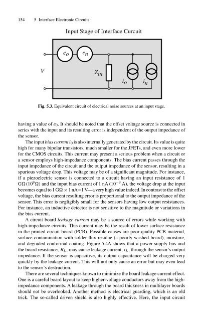
- Page 154 and 155: 136 4 Optical Components of Sensors
- Page 156 and 157: 138 4 Optical Components of Sensors
- Page 158 and 159: 140 4 Optical Components of Sensors
- Page 160 and 161: 142 4 Optical Components of Sensors
- Page 162 and 163: 144 4 Optical Components of Sensors
- Page 164 and 165: 146 4 Optical Components of Sensors
- Page 166 and 167: 148 4 Optical Components of Sensors
- Page 168 and 169: 150 Optical Components of Sensors 1
- Page 170 and 171: 5 Interface Electronic Circuits 5.1
- Page 174 and 175: 5.1 Input Characteristics of Interf
- Page 176 and 177: 5.2 Amplifiers 157 (A) (B) Fig. 5.5
- Page 178 and 179: 5.2 Amplifiers 159 Fig. 5.7. Voltag
- Page 180 and 181: 5.2 Amplifiers 161 (A) (B) Fig. 5.9
- Page 182 and 183: 5.2 Amplifiers 163 Fig. 5.11. An eq
- Page 184 and 185: 5.3 Excitation Circuits 165 5.3.1 C
- Page 186 and 187: 5.3 Excitation Circuits 167 (A) (B)
- Page 188 and 189: 5.3 Excitation Circuits 169 Fig. 5.
- Page 190 and 191: 5.3 Excitation Circuits 171 atures.
- Page 192 and 193: 5.3 Excitation Circuits 173 (A) (B)
- Page 194 and 195: 5.4 Analog-to-Digital Converters 17
- Page 196 and 197: Table 5.2. Binary Bit Weights and R
- Page 198 and 199: 5.4 Analog-to-Digital Converters 17
- Page 200 and 201: 5.4 Analog-to-Digital Converters 18
- Page 202 and 203: 5.4 Analog-to-Digital Converters 18
- Page 204 and 205: 5.4 Analog-to-Digital Converters 18
- Page 206 and 207: 5.5 Direct Digitization and Process
- Page 208 and 209: 5.5 Direct Digitization and Process
- Page 210 and 211: 5.6 Ratiometric Circuits 191 (A) (B
- Page 212 and 213: 5.7 Bridge Circuits 193 determine t
- Page 214 and 215: 5.7 Bridge Circuits 195 Fig. 5.38.
- Page 216 and 217: 5.7 Bridge Circuits 197 Fig. 5.39.
- Page 218 and 219: It can be solved for the temperatur
- Page 220 and 221: 5.8 Data Transmission 201 (A) (B) (
- Page 222 and 223:
5.8 Data Transmission 203 wire meth
- Page 224 and 225:
5.9 Noise in Sensors and Circuits 2
- Page 226 and 227:
5.9 Noise in Sensors and Circuits 2
- Page 228 and 229:
5.9 Noise in Sensors and Circuits 2
- Page 230 and 231:
5.9 Noise in Sensors and Circuits 2
- Page 232 and 233:
5.9 Noise in Sensors and Circuits 2
- Page 234 and 235:
5.9 Noise in Sensors and Circuits 2
- Page 236 and 237:
5.9 Noise in Sensors and Circuits 2
- Page 238 and 239:
5.9 Noise in Sensors and Circuits 2
- Page 240 and 241:
5.9 Noise in Sensors and Circuits 2
- Page 242 and 243:
5.10 Batteries for Low Power Sensor
- Page 244 and 245:
References 225 nickel-metal hydrate
- Page 246 and 247:
6 Occupancy and Motion Detectors Se
- Page 248 and 249:
6.2 Microwave Motion Detectors 229
- Page 250 and 251:
6.2 Microwave Motion Detectors 231
- Page 252 and 253:
6.3 Capacitive Occupancy Detectors
- Page 254 and 255:
6.3 Capacitive Occupancy Detectors
- Page 256 and 257:
6.4 Triboelectric Detectors 237 6.4
- Page 258 and 259:
6.5 Optoelectronic Motion Detectors
- Page 260 and 261:
6.5 Optoelectronic Motion Detectors
- Page 262 and 263:
and the facet pitch is 6.5 Optoelec
- Page 264 and 265:
6.5 Optoelectronic Motion Detectors
- Page 266 and 267:
6.5 Optoelectronic Motion Detectors
- Page 268 and 269:
6.5 Optoelectronic Motion Detectors
- Page 270 and 271:
References 251 Fig. 6.17. Calculate
- Page 272 and 273:
7 Position, Displacement, and Level
- Page 274 and 275:
7.1 Potentiometric Sensors 255 (A)
- Page 276 and 277:
7.2 Gravitational Sensors 257 (A) (
- Page 278 and 279:
7.3 Capacitive Sensors 259 (A) (B)
- Page 280 and 281:
7.3 Capacitive Sensors 261 Fig. 7.7
- Page 282 and 283:
7.4 Inductive and Magnetic Sensors
- Page 284 and 285:
7.4 Inductive and Magnetic Sensors
- Page 286 and 287:
7.4 Inductive and Magnetic Sensors
- Page 288 and 289:
7.4 Inductive and Magnetic Sensors
- Page 290 and 291:
7.4 Inductive and Magnetic Sensors
- Page 292 and 293:
7.4 Inductive and Magnetic Sensors
- Page 294 and 295:
7.5 Optical Sensors 275 Therefore,
- Page 296 and 297:
7.5 Optical Sensors 277 (A) (B) (C)
- Page 298 and 299:
7.5 Optical Sensors 279 (A) (B) Fig
- Page 300 and 301:
7.5 Optical Sensors 281 Fig. 7.32.
- Page 302 and 303:
7.5 Optical Sensors 283 (A) (B) (C)
- Page 304 and 305:
7.5 Optical Sensors 285 is proporti
- Page 306 and 307:
7.6 Ultrasonic Sensors 287 (A) (B)
- Page 308 and 309:
7.7 Radar Sensors 289 (A) (B) Fig.
- Page 310 and 311:
7.7 Radar Sensors 291 (A) (B) Fig.
- Page 312 and 313:
7.8 Thickness and Level Sensors 293
- Page 314 and 315:
7.8 Thickness and Level Sensors 295
- Page 316 and 317:
7.8 Thickness and Level Sensors 297
- Page 318 and 319:
References 299 8. Dakin, J. P., Wad
- Page 320 and 321:
8 Velocity and Acceleration Acceler
- Page 322 and 323:
8.1 Accelerometer Characteristics 3
- Page 324 and 325:
8.2 Capacitive Accelerometers 305 a
- Page 326 and 327:
8.3 Piezoresistive Accelerometers 3
- Page 328 and 329:
8.5 Thermal Accelerometers 309 Fig.
- Page 330 and 331:
8.5 Thermal Accelerometers 311 forc
- Page 332 and 333:
8.6 Gyroscopes 313 8.6 Gyroscopes N
- Page 334 and 335:
8.6 Gyroscopes 315 (A) (B) Fig. 8.1
- Page 336 and 337:
8.6 Gyroscopes 317 Products Company
- Page 338 and 339:
8.7 Piezoelectric Cables 319 (A) (B
- Page 340 and 341:
References 321 (A) (B) Fig. 8.16.Ap
- Page 342 and 343:
9 Force, Strain, and Tactile Sensor
- Page 344 and 345:
9.1 Strain Gauges 325 (A) (B) Fig.
- Page 346 and 347:
9.2 Tactile Sensors 327 9.2 Tactile
- Page 348 and 349:
9.2 Tactile Sensors 329 (A) (B) Fig
- Page 350 and 351:
9.2 Tactile Sensors 331 Fig. 9.7. P
- Page 352 and 353:
9.2 Tactile Sensors 333 Fig. 9.9. T
- Page 354 and 355:
9.3 Piezoelectric Force Sensors 335
- Page 356 and 357:
References 337 14. Karrer, E. and L
- Page 358 and 359:
10 Pressure Sensors “To learn som
- Page 360 and 361:
10.3 Mercury Pressure Sensor 341 1
- Page 362 and 363:
10.4 Bellows, Membranes, and Thin P
- Page 364 and 365:
10.5 Piezoresistive Sensors 345 Fig
- Page 366 and 367:
10.5 Piezoresistive Sensors 347 bri
- Page 368 and 369:
10.6 Capacitive Sensors 349 (A) (B)
- Page 370 and 371:
10.7 VRP Sensors 351 (A) (B) Fig. 1
- Page 372 and 373:
10.8 Optoelectronic Sensors 353 Fig
- Page 374 and 375:
10.9 Vacuum Sensors 355 (A) (B) Fig
- Page 376 and 377:
References 357 (A) (B) (C) Fig. 10.
- Page 378 and 379:
11 Flow Sensors It’s a simple tas
- Page 380 and 381:
11.2 Pressure Gradient Technique 36
- Page 382 and 383:
11.3 Thermal Transport Sensors 363
- Page 384 and 385:
11.3 Thermal Transport Sensors 365
- Page 386 and 387:
11.4 Ultrasonic Sensors 367 A senso
- Page 388 and 389:
11.4 Ultrasonic Sensors 369 Fig. 11
- Page 390 and 391:
induced in the liquid. The magnitud
- Page 392 and 393:
11.6 Microflow Sensors 373 (A) (B)
- Page 394 and 395:
11.7 Breeze Sensor 375 (A) (B) Fig.
- Page 396 and 397:
11.9 Drag Force Flow Sensors 377 Wi
- Page 398 and 399:
References 379 11. Philip-Chandy, R
- Page 400 and 401:
12 Acoustic Sensors “Your ears wi
- Page 402 and 403:
12.3 Fiber-Optic Microphone 383 (A)
- Page 404 and 405:
12.4 Piezoelectric Microphones 385
- Page 406 and 407:
12.5 Electret Microphones 387 Fig.
- Page 408 and 409:
12.6 Solid-State Acoustic Detectors
- Page 410 and 411:
References 391 References 1. Hohm,
- Page 412 and 413:
13 Humidity and Moisture Sensors 13
- Page 414 and 415:
13.1 Concept of Humidity 395 Table
- Page 416 and 417:
13.2 Capacitive Sensors 397 Fig. 13
- Page 418 and 419:
13.3 Electrical Conductivity Sensor
- Page 420 and 421:
13.4 Thermal Conductivity Sensor 40
- Page 422 and 423:
13.6 Oscillating Hygrometer 403 chi
- Page 424 and 425:
References 405 9. Jachowicz, R. S.
- Page 426 and 427:
14 Light Detectors “There is noth
- Page 428 and 429:
14.1 Introduction 409 Table 14.1. B
- Page 430 and 431:
14.2 Photodiodes 411 Maximum revers
- Page 432 and 433:
14.2 Photodiodes 413 when i = 0), w
- Page 434 and 435:
14.2 Photodiodes 415 (A) (B) (C) Fi
- Page 436 and 437:
14.2 Photodiodes 417 Fig. 14.9. Res
- Page 438 and 439:
14.3 Phototransistor 419 Fig. 14.12
- Page 440 and 441:
14.4 Photoresistors 421 (A) (B) Fig
- Page 442 and 443:
14.5 Cooled Detectors 423 (A) (B) F
- Page 444 and 445:
14.6 Thermal Detectors 425 Table 14
- Page 446 and 447:
14.6 Thermal Detectors 427 Fig. 14.
- Page 448 and 449:
Table 14.3. Typical Specifications
- Page 450 and 451:
14.6 Thermal Detectors 431 A dual e
- Page 452 and 453:
14.6 Thermal Detectors 433 Fig. 14.
- Page 454 and 455:
14.6 Thermal Detectors 435 (A) (B)
- Page 456 and 457:
14.6 Thermal Detectors 437 Section
- Page 458 and 459:
14.7 Gas Flame Detectors 439 P = V
- Page 460 and 461:
References 441 housing assures wide
- Page 462 and 463:
15 Radiation Detectors Figure 3.41
- Page 464 and 465:
15.1 Scintillating Detectors 445 Fi
- Page 466 and 467:
15.2 Ionization Detectors 447 emitt
- Page 468 and 469:
15.2 Ionization Detectors 449 Fig.
- Page 470 and 471:
15.2 Ionization Detectors 451 parti
- Page 472 and 473:
15.2 Ionization Detectors 453 There
- Page 474 and 475:
References 455 the pure intrinsic t
- Page 476 and 477:
16 Temperature Sensors When a scien
- Page 478 and 479:
16 Temperature Sensors 459 from whi
- Page 480 and 481:
16.1 Thermoresistive Sensors 461 2.
- Page 482 and 483:
16.1 Thermoresistive Sensors 463 Ta
- Page 484 and 485:
16.1 Thermoresistive Sensors 465 Fi
- Page 486 and 487:
16.1 Thermoresistive Sensors 467 pr
- Page 488 and 489:
16.1 Thermoresistive Sensors 469 Fi
- Page 490 and 491:
16.1 Thermoresistive Sensors 471 Fi
- Page 492 and 493:
16.1 Thermoresistive Sensors 473 Fi
- Page 494 and 495:
16.1 Thermoresistive Sensors 475 (m
- Page 496 and 497:
16.1 Thermoresistive Sensors 477 Fi
- Page 498 and 499:
16.1 Thermoresistive Sensors 479 Fi
- Page 500 and 501:
16.2 Thermoelectric Contact Sensors
- Page 502 and 503:
16.2 Thermoelectric Contact Sensors
- Page 504 and 505:
16.2 Thermoelectric Contact Sensors
- Page 506 and 507:
16.2 Thermoelectric Contact Sensors
- Page 508 and 509:
16.3 Semiconductor P-N Junction Sen
- Page 510 and 511:
16.4 Optical Temperature Sensors 49
- Page 512 and 513:
16.4 Optical Temperature Sensors 49
- Page 514 and 515:
16.5 Acoustic Temperature Sensor 49
- Page 516 and 517:
References 497 plate—the so-calle
- Page 518 and 519:
17 Chemical Sensors 1 Chemical sens
- Page 520 and 521:
17.3 Classification of Chemical-Sen
- Page 522 and 523:
17.4 Direct Sensors 503 17.4 Direct
- Page 524 and 525:
17.4 Direct Sensors 505 voltage e.
- Page 526 and 527:
17.4 Direct Sensors 507 This reacti
- Page 528 and 529:
17.4 Direct Sensors 509 (A) (B) Fig
- Page 530 and 531:
17.4 Direct Sensors 511 µm thick a
- Page 532 and 533:
17.5 Complex Sensors 513 Fig. 17.11
- Page 534 and 535:
17.5 Complex Sensors 515 Fig. 17.12
- Page 536 and 537:
17.5 Complex Sensors 517 frequency
- Page 538 and 539:
Table 17.1. SAW Chemical Sensors 17
- Page 540 and 541:
17.6 Chemical Sensors Versus Instru
- Page 542 and 543:
17.6 Chemical Sensors Versus Instru
- Page 544 and 545:
17.6 Chemical Sensors Versus Instru
- Page 546 and 547:
17.6 Chemical Sensors Versus Instru
- Page 548 and 549:
17.6 Chemical Sensors Versus Instru
- Page 550 and 551:
References 531 13. LaCourse, W.R. P
- Page 552 and 553:
18 Sensor Materials and Technologie
- Page 554 and 555:
18.1 Materials 535 etching is a key
- Page 556 and 557:
18.1 Materials 537 Fig. 18.3. The a
- Page 558 and 559:
18.1 Materials 539 The following is
- Page 560 and 561:
18.1 Materials 541 should be consid
- Page 562 and 563:
18.2 Surface Processing 543 sensor
- Page 564 and 565:
18.2 Surface Processing 545 On a co
- Page 566 and 567:
18.3 Nano-Technology 547 6000-Å la
- Page 568 and 569:
18.3 Nano-Technology 549 exposed to
- Page 570 and 571:
18.3 Nano-Technology 551 Fig. 18.10
- Page 572 and 573:
18.3 Nano-Technology 553 (A) (B) Fi
- Page 574 and 575:
References 555 Fig. 18.17. Bonding
- Page 576 and 577:
Appendix Table A.1. Chemical Symbol
- Page 578 and 579:
Table A.4. SI Conversion Multiples
- Page 580 and 581:
Table A.4 Continued Light cd/in. 2
- Page 582 and 583:
Table A.4 Continued Cup 2.36588 ×
- Page 584 and 585:
Appendix 565 Table A.7. Some Materi
- Page 586 and 587:
Appendix 567 Table A.11. Thermoelec
- Page 588 and 589:
Table A.14. Mechanical Properties o
- Page 590 and 591:
Appendix 571 Table A.18. Typical Em
- Page 592 and 593:
Table A.20. Characteristics of C-Zn
- Page 594 and 595:
Table A.23 Continued Manufacturer P
- Page 596 and 597:
Table A.25. Properties of Glasses S
- Page 598 and 599:
Index α-particles, 443 A/D, 175, 1
- Page 600 and 601:
Index 581 Coulomb’s law, 40 cross
- Page 602 and 603:
Index 583 H 2 O, 108 Hall, 82 Hall
- Page 604 and 605:
Index 585 occupancy sensors, 227 od
- Page 606 and 607:
Index 587 SAW, 75, 388, 404, 496, 5
- Page 608:
Index 589 velocity sensor, 302 vert