- Page 1 and 2:
Frequency
- Page 3 and 4:
Warning!Dangerous electrical voltag
- Page 5 and 6:
04/07 AWB8230-1541GBContentsAbout t
- Page 7 and 8:
04/07 AWB8230-1541GB ContentsPID co
- Page 9 and 10:
04/07 AWB8230-1541GBAbout this manu
- Page 11 and 12:
PRG ENTERPRG ENTER04/07 AWB8230-154
- Page 13 and 14:
PRG ENTER04/07 AWB8230-1541GB Ratin
- Page 15 and 16:
I O04/07 AWB8230-1541GB Layout of t
- Page 17 and 18:
04/07 AWB8230-1541GB Selection crit
- Page 19 and 20:
04/07 AWB8230-1541GB2 EngineeringTh
- Page 21 and 22:
04/07 AWB8230-1541GB Performance fe
- Page 23 and 24:
04/07 AWB8230-1541GB Connection to
- Page 25 and 26:
04/07 AWB8230-1541GB EMC co
- Page 27 and 28:
04/07 AWB8230-1541GB Motor and circ
- Page 29 and 30:
04/07 AWB8230-1541GB BrakingBypass
- Page 31 and 32:
04/07 AWB8230-1541GB BrakingPK PD:
- Page 33 and 34:
04/07 AWB8230-1541GB3 InstallationT
- Page 35 and 36:
PRG ENTER04/07 AWB8230-1541GB Fitti
- Page 37 and 38:
POWERALARMHzARUNPRG04/07 AWB8230-15
- Page 39 and 40:
04/07 AWB8230-1541GB EMC-co
- Page 41 and 42:
PRG ENTERI O04/07 AWB8230-1541GB El
- Page 43 and 44:
04/07 AWB8230-1541GB Electrical con
- Page 45 and 46:
04/07 AWB8230-1541GB Electrical con
- Page 47 and 48:
04/07 AWB8230-1541GB Electrical con
- Page 49 and 50:
04/07 AWB8230-1541GB Electrical con
- Page 51 and 52:
04/07 AWB8230-1541GB Electrical con
- Page 53 and 54:
04/07 AWB8230-1541GB4 Using the DF5
- Page 55 and 56:
I O04/07 AWB8230-1541GB Initial sta
- Page 57 and 58:
04/07 AWB8230-1541GB Initial starti
- Page 59 and 60:
04/07 AWB8230-1541GB KeypadKeypadTh
- Page 61 and 62:
04/07 AWB8230-1541GB KeypadQuick pa
- Page 63 and 64:
04/07 AWB8230-1541GB KeypadExamples
- Page 65 and 66:
04/07 AWB8230-1541GB KeypadSelf-adh
- Page 67 and 68:
04/07 AWB8230-1541GB KeypadPOWERHzA
- Page 69 and 70:
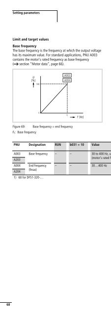
04/07 AWB8230-1541GB5 Setting param
- Page 71 and 72:
04/07 AWB8230-1541GB Motor controlM
- Page 73 and 74:
04/07 AWB8230-1541GB Motor controlI
- Page 75 and 76:
I O04/07 AWB8230-1541GB Reference a
- Page 77 and 78:
04/07 AWB8230-1541GB Reference and
- Page 79 and 80:
04/07 AWB8230-1541GB Reference and
- Page 81 and 82:
04/07 AWB8230-1541GB Reference and
- Page 83 and 84:
04/07 AWB8230-1541GB Reference and
- Page 85 and 86:
04/07 AWB8230-1541GB Reference and
- Page 87 and 88:
04/07 AWB8230-1541GB Reference and
- Page 89 and 90:
04/07 AWB8230-1541GB Reference and
- Page 91 and 92: 04/07 AWB8230-1541GB Reference and
- Page 93 and 94: ’04/07 AWB8230-1541GB Reference a
- Page 95 and 96: 04/07 AWB8230-1541GB Reference and
- Page 97 and 98: 04/07 AWB8230-1541GB Reference and
- Page 99 and 100: 04/07 AWB8230-1541GB Reference and
- Page 101 and 102: 04/07 AWB8230-1541GB Reference and
- Page 103 and 104: 04/07 AWB8230-1541GB Reference and
- Page 105 and 106: 04/07 AWB8230-1541GB Reference and
- Page 107 and 108: 04/07 AWB8230-1541GB Reference and
- Page 109 and 110: 04/07 AWB8230-1541GB Actual value a
- Page 111 and 112: 04/07 AWB8230-1541GB Actual value a
- Page 113 and 114: 04/07 AWB8230-1541GB Actual value a
- Page 115 and 116: 04/07 AWB8230-1541GB Actual value a
- Page 117 and 118: 04/07 AWB8230-1541GB Monitoring fun
- Page 119 and 120: 04/07 AWB8230-1541GB Monitoring fun
- Page 121 and 122: 04/07 AWB8230-1541GB Monitoring fun
- Page 123 and 124: 04/07 AWB8230-1541GB Monitoring fun
- Page 125 and 126: 04/07 AWB8230-1541GB BrakingBraking
- Page 127 and 128: 04/07 AWB8230-1541GB Mathematical a
- Page 129 and 130: 04/07 AWB8230-1541GB Mathematical a
- Page 131 and 132: 04/07 AWB8230-1541GB PID controlPID
- Page 133 and 134: 04/07 AWB8230-1541GB PID controlPNU
- Page 135 and 136: 04/07 AWB8230-1541GB PID controlAct
- Page 137 and 138: 04/07 AWB8230-1541GB PID controlInv
- Page 139 and 140: 04/07 AWB8230-1541GB System setting
- Page 141: 04/07 AWB8230-1541GB System setting
- Page 145 and 146: 04/07 AWB8230-1541GB System setting
- Page 147 and 148: PRG ENTER04/07 AWB8230-1541GB6 Seri
- Page 149 and 150: I O04/07 AWB8230-1541GB Setting the
- Page 151 and 152: 04/07 AWB8230-1541GB Displayed valu
- Page 153 and 154: 04/07 AWB8230-1541GB The network pr
- Page 155 and 156: 04/07 AWB8230-1541GB The network pr
- Page 157 and 158: 04/07 AWB8230-1541GB The network pr
- Page 159 and 160: 04/07 AWB8230-1541GB The network pr
- Page 161 and 162: 04/07 AWB8230-1541GB Modbus registe
- Page 163 and 164: 04/07 AWB8230-1541GB Holding regist
- Page 165 and 166: 04/07 AWB8230-1541GB Holding regist
- Page 167 and 168: 04/07 AWB8230-1541GB Holding regist
- Page 169 and 170: 04/07 AWB8230-1541GB Holding regist
- Page 171 and 172: 04/07 AWB8230-1541GB Holding regist
- Page 173 and 174: 04/07 AWB8230-1541GB Holding regist
- Page 175 and 176: 04/07 AWB8230-1541GB Holding regist
- Page 177 and 178: 04/07 AWB8230-1541GB Holding regist
- Page 179 and 180: 04/07 AWB8230-1541GB Holding regist
- Page 181 and 182: 04/07 AWB8230-1541GB Holding regist
- Page 183 and 184: 04/07 AWB8230-1541GB Holding regist
- Page 185 and 186: 04/07 AWB8230-1541GB7 Error message
- Page 187 and 188: 04/07 AWB8230-1541GB Fault signal (
- Page 189 and 190: 04/07 AWB8230-1541GB Automatic rest
- Page 191 and 192: 04/07 AWB8230-1541GB Troubleshootin
- Page 193 and 194:
04/07 AWB8230-1541GB8 Maintenance a
- Page 195 and 196:
04/07 AWB8230-1541GB Service life o
- Page 197 and 198:
04/07 AWB8230-1541GBAppendixSpecial
- Page 199 and 200:
04/07 AWB8230-1541GBDF51-340 device
- Page 201 and 202:
04/07 AWB8230-1541GB Weights and di
- Page 203 and 204:
PRG ENTER04/07 AWB8230-1541GB Optio
- Page 205 and 206:
04/07 AWB8230-1541GB Optional modul
- Page 207 and 208:
04/07 AWB8230-1541GB Optional modul
- Page 209 and 210:
04/07 AWB8230-1541GB Optional modul
- Page 211 and 212:
04/07 AWB8230-1541GB Optional modul
- Page 213 and 214:
04/07 AWB8230-1541GB Optional modul
- Page 215 and 216:
PRG ENTERPRG ENTER04/07 AWB8230-154
- Page 217 and 218:
04/07 AWB8230-1541GB Operating soft
- Page 219 and 220:
04/07 AWB8230-1541GB Operating soft
- Page 221 and 222:
04/07 AWB8230-1541GB Tightening tor
- Page 223 and 224:
04/07 AWB8230-1541GB RFI filtersU1V
- Page 225 and 226:
04/07 AWB8230-1541GB Mains contacto
- Page 227 and 228:
04/07 AWB8230-1541GB Motor reactorM
- Page 229 and 230:
04/07 AWB8230-1541GB Sine-wave filt
- Page 231 and 232:
04/07 AWB8230-1541GB UL ® Caution,
- Page 233 and 234:
04/07 AWB8230-1541GBParameter listA
- Page 235 and 236:
04/07 AWB8230-1541GB Parameter list
- Page 237 and 238:
04/07 AWB8230-1541GB Parameter list
- Page 239 and 240:
04/07 AWB8230-1541GB Parameter list
- Page 241 and 242:
04/07 AWB8230-1541GB Parameter list
- Page 243 and 244:
04/07 AWB8230-1541GB Parameter list
- Page 245 and 246:
04/07 AWB8230-1541GB Parameter list
- Page 247 and 248:
04/07 AWB8230-1541GB Parameter list
- Page 249 and 250:
04/07 AWB8230-1541GB Parameter list
- Page 251 and 252:
04/07 AWB8230-1541GBIndexA Alphabet
- Page 253:
04/07 AWB8230-1541GB IndexPIDPID co