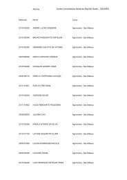
80C186EB/80C188EB Microprocessor User's Manual - CEUNES
80C186EB/80C188EB Microprocessor User's Manual - CEUNES
80C186EB/80C188EB Microprocessor User's Manual - CEUNES

Create successful ePaper yourself
Turn your PDF publications into a flip-book with our unique Google optimized e-Paper software.
CONTENTSFIGURESFigurePage3-15 Generating a Normally Not-Ready Bus Signal ...........................................................3-163-16 Generating a Normally Ready Bus Signal..................................................................3-173-17 Normally Not-Ready System Timing ..........................................................................3-183-18 Normally Ready System Timings ...............................................................................3-193-19 Typical Read Bus Cycle .............................................................................................3-213-20 Read-Only Device Interface .......................................................................................3-223-21 Typical Write Bus Cycle..............................................................................................3-233-22 16-Bit Bus Read/Write Device Interface.....................................................................3-243-23 Interrupt Acknowledge Bus Cycle...............................................................................3-263-24 Typical 82C59A Interface ...........................................................................................3-273-25 HALT Bus Cycle .........................................................................................................3-303-26 Returning to HALT After a HOLD/HLDA Bus Exchange ............................................3-313-27 Returning to HALT After a Refresh Bus Cycle ...........................................................3-323-28 Exiting HALT (Powerdown Mode) ..............................................................................3-333-29 Exiting HALT (Active/Idle Mode).................................................................................3-343-30 DEN and DT/R Timing Relationships .........................................................................3-353-31 Buffered AD Bus System............................................................................................3-363-32 Qualifying DEN with Chip-Selects ..............................................................................3-373-33 Timing Sequence Entering HOLD ..............................................................................3-403-34 Refresh Request During HOLD..................................................................................3-423-35 Latching HLDA ...........................................................................................................3-433-36 Exiting HOLD..............................................................................................................3-444-1 PCB Relocation Register..............................................................................................4-25-1 Clock Generator ...........................................................................................................5-15-2 Ideal Operation of Pierce Oscillator..............................................................................5-25-3 Crystal Connections to <strong>Microprocessor</strong>........................................................................5-35-4 Equations for Crystal Calculations................................................................................5-45-5 Simple RC Circuit for Powerup Reset ..........................................................................5-75-6 Cold Reset Waveform ..................................................................................................5-85-7 Warm Reset Waveform ................................................................................................5-95-8 Clock Synchronization at Reset..................................................................................5-105-9 Power Control Register ..............................................................................................5-125-10 Entering Idle Mode .....................................................................................................5-135-11 HOLD/HLDA During Idle Mode...................................................................................5-145-12 Entering Powerdown Mode ........................................................................................5-175-13 Powerdown Timer Circuit ...........................................................................................5-186-1 Common Chip-Select Generation Methods..................................................................6-26-2 Chip-Select Block Diagram...........................................................................................6-36-3 Chip-Select Relative Timings .......................................................................................6-46-4 UCS Reset Configuration .............................................................................................6-56-5 START Register Definition ...........................................................................................6-76-6 STOP Register Definition .............................................................................................6-86-7 Wait State and Ready Control Functions ...................................................................6-126-8 Overlapping Chip-Selects...........................................................................................6-13xi