80C186EB/80C188EB Microprocessor User's Manual - CEUNES
80C186EB/80C188EB Microprocessor User's Manual - CEUNES
80C186EB/80C188EB Microprocessor User's Manual - CEUNES

Create successful ePaper yourself
Turn your PDF publications into a flip-book with our unique Google optimized e-Paper software.
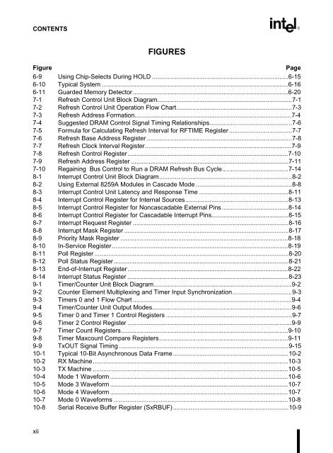
CONTENTSFIGURESFigurePage6-9 Using Chip-Selects During HOLD ..............................................................................6-156-10 Typical System ...........................................................................................................6-166-11 Guarded Memory Detector.........................................................................................6-207-1 Refresh Control Unit Block Diagram.............................................................................7-17-2 Refresh Control Unit Operation Flow Chart..................................................................7-37-3 Refresh Address Formation..........................................................................................7-47-4 Suggested DRAM Control Signal Timing Relationships...............................................7-67-5 Formula for Calculating Refresh Interval for RFTIME Register....................................7-77-6 Refresh Base Address Register ...................................................................................7-87-7 Refresh Clock Interval Register....................................................................................7-97-8 Refresh Control Register............................................................................................7-107-9 Refresh Address Register ..........................................................................................7-117-10 Regaining Bus Control to Run a DRAM Refresh Bus Cycle......................................7-148-1 Interrupt Control Unit Block Diagram............................................................................8-28-2 Using External 8259A Modules in Cascade Mode .......................................................8-88-3 Interrupt Control Unit Latency and Response Time ...................................................8-118-4 Interrupt Control Register for Internal Sources...........................................................8-138-5 Interrupt Control Register for Noncascadable External Pins......................................8-148-6 Interrupt Control Register for Cascadable Interrupt Pins............................................8-158-7 Interrupt Request Register .........................................................................................8-168-8 Interrupt Mask Register ..............................................................................................8-178-9 Priority Mask Register ................................................................................................8-188-10 In-Service Register.....................................................................................................8-198-11 Poll Register ...............................................................................................................8-208-12 Poll Status Register....................................................................................................8-218-13 End-of-Interrupt Register............................................................................................8-228-14 Interrupt Status Register ............................................................................................8-239-1 Timer/Counter Unit Block Diagram...............................................................................9-29-2 Counter Element Multiplexing and Timer Input Synchronization..................................9-39-3 Timers 0 and 1 Flow Chart ...........................................................................................9-49-4 Timer/Counter Unit Output Modes................................................................................9-69-5 Timer 0 and Timer 1 Control Registers ........................................................................9-79-6 Timer 2 Control Register ..............................................................................................9-99-7 Timer Count Registers................................................................................................9-109-8 Timer Maxcount Compare Registers..........................................................................9-119-9 TxOUT Signal Timing .................................................................................................9-1510-1 Typical 10-Bit Asynchronous Data Frame..................................................................10-210-2 RX Machine................................................................................................................10-310-3 TX Machine ................................................................................................................10-510-4 Mode 1 Waveform ......................................................................................................10-610-5 Mode 3 Waveform ......................................................................................................10-710-6 Mode 4 Waveform ......................................................................................................10-710-7 Mode 0 Waveforms ....................................................................................................10-810-8 Serial Receive Buffer Register (SxRBUF)..................................................................10-9xii