- Page 1 and 2:
80C186EB/80C188EBMicroprocessorUser
- Page 3 and 4:
Information in this document is pro
- Page 5 and 6:
CONTENTS2.3.2 Software Interrupts .
- Page 7 and 8:
CONTENTS6.4.4 Enabling and Disablin
- Page 9 and 10:
CONTENTS10.2.2 Asynchronous Mode Pr
- Page 11 and 12:
CONTENTSFIGURESFigurePage2-1 Simpli
- Page 13 and 14:
CONTENTSFIGURESFigurePage6-9 Using
- Page 15 and 16:
CONTENTSTableTABLESPage1-1 Comparis
- Page 17 and 18:
CONTENTSEXAMPLESExamplePage5-1 Init
- Page 20 and 21:
CHAPTER 1INTRODUCTIONThe 8086 micro
- Page 22 and 23:
INTRODUCTIONEach chapter covers a s
- Page 24 and 25:
INTRODUCTION1.3.1 How to Use Intel'
- Page 26:
Overview of the80C186 FamilyArchite
- Page 29 and 30:
OVERVIEW OF THE 80C186 FAMILY ARCHI
- Page 31 and 32:
OVERVIEW OF THE 80C186 FAMILY ARCHI
- Page 33 and 34:
OVERVIEW OF THE 80C186 FAMILY ARCHI
- Page 35 and 36:
OVERVIEW OF THE 80C186 FAMILY ARCHI
- Page 37 and 38:
OVERVIEW OF THE 80C186 FAMILY ARCHI
- Page 39:
OVERVIEW OF THE 80C186 FAMILY ARCHI
- Page 42 and 43:
OVERVIEW OF THE 80C186 FAMILY ARCHI
- Page 44 and 45:
OVERVIEW OF THE 80C186 FAMILY ARCHI
- Page 46 and 47:
OVERVIEW OF THE 80C186 FAMILY ARCHI
- Page 48 and 49:
OVERVIEW OF THE 80C186 FAMILY ARCHI
- Page 50 and 51:
OVERVIEW OF THE 80C186 FAMILY ARCHI
- Page 52 and 53:
OVERVIEW OF THE 80C186 FAMILY ARCHI
- Page 54 and 55:
OVERVIEW OF THE 80C186 FAMILY ARCHI
- Page 56 and 57:
OVERVIEW OF THE 80C186 FAMILY ARCHI
- Page 58 and 59:
OVERVIEW OF THE 80C186 FAMILY ARCHI
- Page 60 and 61:
OVERVIEW OF THE 80C186 FAMILY ARCHI
- Page 62 and 63:
OVERVIEW OF THE 80C186 FAMILY ARCHI
- Page 64 and 65:
OVERVIEW OF THE 80C186 FAMILY ARCHI
- Page 66 and 67:
OVERVIEW OF THE 80C186 FAMILY ARCHI
- Page 68 and 69:
OVERVIEW OF THE 80C186 FAMILY ARCHI
- Page 70 and 71:
OVERVIEW OF THE 80C186 FAMILY ARCHI
- Page 72 and 73:
OVERVIEW OF THE 80C186 FAMILY ARCHI
- Page 74 and 75:
OVERVIEW OF THE 80C186 FAMILY ARCHI
- Page 76 and 77:
OVERVIEW OF THE 80C186 FAMILY ARCHI
- Page 78:
Bus Interface Unit3
- Page 81 and 82:
BUS INTERFACE UNITPhysical Implemen
- Page 83 and 84:
BUS INTERFACE UNIT(X + 1)(X)A19:1 D
- Page 85 and 86:
BUS INTERFACE UNITFor word transfer
- Page 87 and 88:
BUS INTERFACE UNITCLKOUTT4 T1 T2 T3
- Page 89 and 90:
BUS INTERFACE UNITCLKOUTT4or TI T1
- Page 91 and 92:
BUS INTERFACE UNITSignals From CPU4
- Page 93 and 94:
BUS INTERFACE UNITT2T3or TWT4or TIC
- Page 95 and 96:
BUS INTERFACE UNITA normally not-re
- Page 97 and 98:
BUS INTERFACE UNITT2or T3or TWT3or
- Page 99 and 100:
BUS INTERFACE UNITAn idle bus state
- Page 101 and 102:
BUS INTERFACE UNIT3.5.1.1 Refresh B
- Page 103 and 104:
BUS INTERFACE UNITMost memory and p
- Page 105 and 106:
BUS INTERFACE UNITCLKOUTT4 T2 T3 TI
- Page 107 and 108:
BUS INTERFACE UNIT3.5.4 HALT Bus Cy
- Page 109 and 110:
BUS INTERFACE UNITCLKOUTT1 TI TIALE
- Page 111 and 112:
BUS INTERFACE UNITCLKOUTALES2:0AD15
- Page 113 and 114:
BUS INTERFACE UNITCLKOUTNMI/INTxNot
- Page 115 and 116:
BUS INTERFACE UNITALEProcessorA19:1
- Page 117 and 118:
BUS INTERFACE UNITThe WAIT instruct
- Page 119 and 120:
BUS INTERFACE UNITCLKOUTHOLD124HLDA
- Page 121 and 122:
BUS INTERFACE UNITCLKOUT1 3 4HOLDHL
- Page 123 and 124:
BUS INTERFACE UNITCLKOUTHOLD12345HL
- Page 126:
Peripheral ControlBlock4
- Page 129 and 130:
PERIPHERAL CONTROL BLOCKRegister Na
- Page 131 and 132:
PERIPHERAL CONTROL BLOCK4.3 RESERVE
- Page 133 and 134:
PERIPHERAL CONTROL BLOCK4.4.3.1 Wri
- Page 135 and 136:
PERIPHERAL CONTROL BLOCK4-8
- Page 138 and 139:
CHAPTER 5CLOCK GENERATION AND POWER
- Page 140 and 141:
CLOCK GENERATION AND POWER MANAGEME
- Page 142 and 143:
CLOCK GENERATION AND POWER MANAGEME
- Page 144 and 145:
CLOCK GENERATION AND POWER MANAGEME
- Page 146 and 147:
CLOCK GENERATION AND POWER MANAGEME
- Page 148 and 149:
CLOCK GENERATION AND POWER MANAGEME
- Page 150 and 151:
CLOCK GENERATION AND POWER MANAGEME
- Page 152 and 153:
CLOCK GENERATION AND POWER MANAGEME
- Page 154 and 155:
CLOCK GENERATION AND POWER MANAGEME
- Page 156 and 157:
CLOCK GENERATION AND POWER MANAGEME
- Page 158:
Chip-Select Unit6
- Page 161 and 162:
CHIP-SELECT UNIT27C25674AC138A1:13A
- Page 163 and 164:
CHIP-SELECT UNITT4 T1 T2 T3T4CLKOUT
- Page 165 and 166:
CHIP-SELECT UNITThe START register
- Page 167 and 168:
CHIP-SELECT UNITRegister Name:Regis
- Page 169 and 170:
CHIP-SELECT UNIT6.4.2 Start Address
- Page 171 and 172:
CHIP-SELECT UNITBUS READYREADY Cont
- Page 173 and 174:
CHIP-SELECT UNITTable 6-3 lists exa
- Page 175 and 176:
CHIP-SELECT UNITREADYALEA19:16AD15:
- Page 177 and 178:
CHIP-SELECT UNITDRAM_BASEEQU 128 ;W
- Page 179 and 180:
CHIP-SELECT UNIT; DATA SEGMENTDATAS
- Page 182 and 183:
CHAPTER 7REFRESH CONTROL UNITThe Re
- Page 184 and 185:
REFRESH CONTROL UNITRefresh Control
- Page 186 and 187:
REFRESH CONTROL UNIT7.5 REFRESH BUS
- Page 188 and 189:
REFRESH CONTROL UNIT7.7 PROGRAMMING
- Page 190 and 191:
REFRESH CONTROL UNITRegister Name:R
- Page 192 and 193:
REFRESH CONTROL UNITRegister Name:R
- Page 194 and 195:
REFRESH CONTROL UNITmov dx, RFBASEm
- Page 196:
Interrupt ControlUnit8
- Page 199 and 200:
INTERRUPT CONTROL UNITTimer 0 Timer
- Page 201 and 202:
INTERRUPT CONTROL UNITInterrupt sou
- Page 203 and 204:
INTERRUPT CONTROL UNIT8.2.2.1 Prior
- Page 205 and 206:
INTERRUPT CONTROL UNITINTINT08259Ao
- Page 207 and 208:
INTERRUPT CONTROL UNIT8.2.6 Edge an
- Page 209 and 210:
INTERRUPT CONTROL UNITTable 8-3. In
- Page 211 and 212:
INTERRUPT CONTROL UNIT.Register Nam
- Page 213 and 214:
INTERRUPT CONTROL UNIT8.3.2 Interru
- Page 215 and 216:
INTERRUPT CONTROL UNIT8.3.4 Priorit
- Page 217 and 218:
INTERRUPT CONTROL UNITReading the P
- Page 219 and 220:
INTERRUPT CONTROL UNITRegister Name
- Page 221 and 222:
INTERRUPT CONTROL UNIT3. Program th
- Page 224 and 225:
CHAPTER 9TIMER/COUNTER UNITThe Time
- Page 226 and 227:
TIMER/COUNTER UNITTimer 0 Timer 1 T
- Page 228 and 229:
TIMER/COUNTER UNITContinued From"A"
- Page 230 and 231:
TIMER/COUNTER UNITRegister Name:Reg
- Page 232 and 233:
TIMER/COUNTER UNITRegister Name:Reg
- Page 234 and 235:
TIMER/COUNTER UNITRegister Name:Reg
- Page 236 and 237:
TIMER/COUNTER UNITThe timer countin
- Page 238 and 239:
TIMER/COUNTER UNITTimer 0Serviced1I
- Page 240 and 241:
TIMER/COUNTER UNIT9.3.2 Synchroniza
- Page 242 and 243:
TIMER/COUNTER UNITlib_80186 segment
- Page 244 and 245:
TIMER/COUNTER UNIT$mod186nameexampl
- Page 246 and 247:
TIMER/COUNTER UNIT_CMPB equ word pt
- Page 248: SerialCommunicationsUnit10
- Page 251 and 252: SERIAL COMMUNICATIONS UNIT1 2 3 4 5
- Page 253 and 254: SERIAL COMMUNICATIONS UNITThe RX ma
- Page 255 and 256: SERIAL COMMUNICATIONS UNITThe Trans
- Page 257 and 258: SERIAL COMMUNICATIONS UNIT5. At the
- Page 259 and 260: SERIAL COMMUNICATIONS UNITRegister
- Page 261 and 262: SERIAL COMMUNICATIONS UNITRegister
- Page 263 and 264: SERIAL COMMUNICATIONS UNIT3. If the
- Page 265 and 266: SERIAL COMMUNICATIONS UNITThe seria
- Page 267 and 268: SERIAL COMMUNICATIONS UNIT10.2.3 Pr
- Page 269 and 270: SERIAL COMMUNICATIONS UNITBCLK is a
- Page 271 and 272: SERIAL COMMUNICATIONS UNITChannel_0
- Page 273 and 274: SERIAL COMMUNICATIONS UNITmovmovmov
- Page 275 and 276: SERIAL COMMUNICATIONS UNIT10.5.2 Mo
- Page 277 and 278: SERIAL COMMUNICATIONS UNITMASTER186
- Page 279 and 280: SERIAL COMMUNICATIONS UNIT$mod186na
- Page 281 and 282: SERIAL COMMUNICATIONS UNIT$mod186na
- Page 283 and 284: SERIAL COMMUNICATIONS UNITcmp al, F
- Page 285 and 286: SERIAL COMMUNICATIONS UNIT10-36
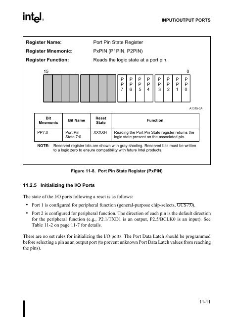
- Page 288 and 289: CHAPTER 11INPUT/OUTPUT PORTSMany ap
- Page 290 and 291: INPUT/OUTPUT PORTS11.1.2 Input Port
- Page 292 and 293: INPUT/OUTPUT PORTSFrom IntegratedPe
- Page 294 and 295: INPUT/OUTPUT PORTS11.1.5.1 Port 1 O
- Page 296 and 297: INPUT/OUTPUT PORTSRegister Name:Reg
- Page 300: Math Coprocessing12
- Page 303 and 304: MATH COPROCESSING12.3 THE 80C187 MA
- Page 305 and 306: MATH COPROCESSINGAvailable data typ
- Page 307 and 308: MATH COPROCESSING12.3.1.5 Constant
- Page 309 and 310: MATH COPROCESSINGIncreasing Signifi
- Page 311 and 312: MATH COPROCESSING12.4.1 Clocking th
- Page 313 and 314: MATH COPROCESSINGExternalOscillator
- Page 315 and 316: MATH COPROCESSING80C186Modular Core
- Page 317 and 318: MATH COPROCESSING$mod186$modc187nam
- Page 320 and 321: CHAPTER 13ONCE MODEONCE (pronounced
- Page 322: 80C186 InstructionSet Additions and
- Page 325 and 326: 80C186 INSTRUCTION SET ADDITIONS AN
- Page 327 and 328: 80C186 INSTRUCTION SET ADDITIONS AN
- Page 329 and 330: 80C186 INSTRUCTION SET ADDITIONS AN
- Page 331 and 332: 80C186 INSTRUCTION SET ADDITIONS AN
- Page 333 and 334: 80C186 INSTRUCTION SET ADDITIONS AN
- Page 336 and 337: APPENDIX BINPUT SYNCHRONIZATIONMany
- Page 338: Instruction SetDescriptionsC
- Page 341 and 342: INSTRUCTION SET DESCRIPTIONSTable C
- Page 343 and 344: INSTRUCTION SET DESCRIPTIONSTable C
- Page 345 and 346: INSTRUCTION SET DESCRIPTIONSTable C
- Page 347 and 348: INSTRUCTION SET DESCRIPTIONSTable C
- Page 349 and 350:
INSTRUCTION SET DESCRIPTIONSTable C
- Page 351 and 352:
INSTRUCTION SET DESCRIPTIONSTable C
- Page 353 and 354:
INSTRUCTION SET DESCRIPTIONSTable C
- Page 355 and 356:
INSTRUCTION SET DESCRIPTIONSTable C
- Page 357 and 358:
INSTRUCTION SET DESCRIPTIONSINCINST
- Page 359 and 360:
INSTRUCTION SET DESCRIPTIONSTable C
- Page 361 and 362:
INSTRUCTION SET DESCRIPTIONSTable C
- Page 363 and 364:
INSTRUCTION SET DESCRIPTIONSTable C
- Page 365 and 366:
INSTRUCTION SET DESCRIPTIONSTable C
- Page 367 and 368:
INSTRUCTION SET DESCRIPTIONSTable C
- Page 369 and 370:
INSTRUCTION SET DESCRIPTIONSTable C
- Page 371 and 372:
INSTRUCTION SET DESCRIPTIONSOROUTTa
- Page 373 and 374:
INSTRUCTION SET DESCRIPTIONSTable C
- Page 375 and 376:
INSTRUCTION SET DESCRIPTIONSTable C
- Page 377 and 378:
INSTRUCTION SET DESCRIPTIONSTable C
- Page 379 and 380:
INSTRUCTION SET DESCRIPTIONSTable C
- Page 381 and 382:
INSTRUCTION SET DESCRIPTIONSTable C
- Page 383 and 384:
INSTRUCTION SET DESCRIPTIONSTable C
- Page 385 and 386:
INSTRUCTION SET DESCRIPTIONSTable C
- Page 387 and 388:
INSTRUCTION SET DESCRIPTIONSC-48
- Page 390 and 391:
APPENDIX DINSTRUCTION SET OPCODESAN
- Page 392 and 393:
INSTRUCTION SET OPCODES AND CLOCK C
- Page 394 and 395:
INSTRUCTION SET OPCODES AND CLOCK C
- Page 396 and 397:
INSTRUCTION SET OPCODES AND CLOCK C
- Page 398 and 399:
INSTRUCTION SET OPCODES AND CLOCK C
- Page 400 and 401:
INSTRUCTION SET OPCODES AND CLOCK C
- Page 402 and 403:
INSTRUCTION SET OPCODES AND CLOCK C
- Page 404 and 405:
INSTRUCTION SET OPCODES AND CLOCK C
- Page 406 and 407:
INSTRUCTION SET OPCODES AND CLOCK C
- Page 408 and 409:
INSTRUCTION SET OPCODES AND CLOCK C
- Page 410 and 411:
INSTRUCTION SET OPCODES AND CLOCK C
- Page 412:
Index
- Page 415 and 416:
INDEXand T-states, 3-9data phase, 3
- Page 417 and 418:
INDEXarithmetic instructions, 2-19-
- Page 419 and 420:
INDEXblock diagram, 3-15implementat
- Page 421:
INDEXWWait statesand bus cycles, 3-