- Page 1 and 2:
A PHYSICAL IMPLEMENTATION WITH CUST
- Page 3 and 4:
A PHYSICAL IMPLEMENTATION WITH CUST
- Page 5 and 6:
4.0 ASIC DESIGN FLOW ..............
- Page 7 and 8:
6.5.5 Characterization Results for
- Page 9 and 10:
LIST OF TABLES Table 5-1: ALU Modul
- Page 11 and 12:
LIST OF FIGURES Figure 1-1: SuperCI
- Page 13 and 14:
Figure 5-20: BIGFABRIC Logical Diag
- Page 15 and 16:
Figure 7-4: EEPROM Erase Physical O
- Page 17 and 18:
ACKNOWLEDGEMENTS “Many, O Jehovah
- Page 19 and 20:
1.0 INTRODUCTION Technological adva
- Page 21 and 22:
Property) block. The physical desig
- Page 23 and 24:
the thesis proposes a power gated m
- Page 25 and 26:
2.0 SUPERCISC RECONFIGURABLE HARDWA
- Page 27 and 28:
The specifications of the hardware
- Page 29 and 30:
INP2 selects from ALU1, ALU2, ALU3
- Page 31 and 32:
3.0 POWER ESTIMATION The need for e
- Page 33 and 34:
3.1.1 Static Power Consumption Stat
- Page 35 and 36:
Internal Power Internal Power is th
- Page 37 and 38:
Switching activity Generation Switc
- Page 39 and 40:
Figure 3-4: Leakage Power definitio
- Page 41 and 42:
The entire array contains informati
- Page 43 and 44:
3.3.2 Calculation of Fall Power Fig
- Page 45 and 46:
Figure 3-10: Off-state leakage Powe
- Page 47 and 48:
Figure 4-1 : Typical ASIC Design Fl
- Page 49 and 50:
Figure 4-2: ASIC Physical Design Fl
- Page 51 and 52:
4.1.2 Powerplanning Power planning
- Page 53 and 54:
created in the design. Routing feed
- Page 55 and 56:
4.1.7 Routing Once the standard cel
- Page 57 and 58:
Table 5-1: ALU Module Specification
- Page 59 and 60:
Table 5-2 shows the important speci
- Page 61 and 62:
the basic parameters are specified,
- Page 63 and 64:
direction have to be aligned on the
- Page 65 and 66:
ALU Stripe Pin Assignment The “ib
- Page 67 and 68:
5.2.1 MUX Module Specifications As
- Page 69 and 70:
Figure 5-12: MUX Stripe Logical Dia
- Page 71 and 72:
MUX initialization routine The MUX
- Page 73 and 74: Table 5-10: MUX Stripe Pin Placemen
- Page 75 and 76: Figure 5-15: FINALMUX Module Logica
- Page 77 and 78: Table 5-12: Final MUX Stripe Specif
- Page 79 and 80: pins in the FINALMUX stripe is plac
- Page 81 and 82: larger system. Figure 5-22 shows th
- Page 83 and 84: Figure 5-20: BIGFABRIC Logical Diag
- Page 85 and 86: Figure 5-22: Place and Routed BIGFA
- Page 87 and 88: BIGFABRIC Stripe Pin Assignment As
- Page 89 and 90: The SPEF file can be generated usin
- Page 91 and 92: 5.5.1 Power Results for ADPCM Encod
- Page 93 and 94: 5.5.3 Power Results for IDCT Row Be
- Page 95 and 96: 5.5.5 Power Results for Sobel Bench
- Page 97 and 98: 6.0 DELAY ELEMENTS FOR LOW POWER FA
- Page 99 and 100: Transmission gate with Schmitt Trig
- Page 101 and 102: PMOS transistors have their gate in
- Page 103 and 104: output normally. The signal integri
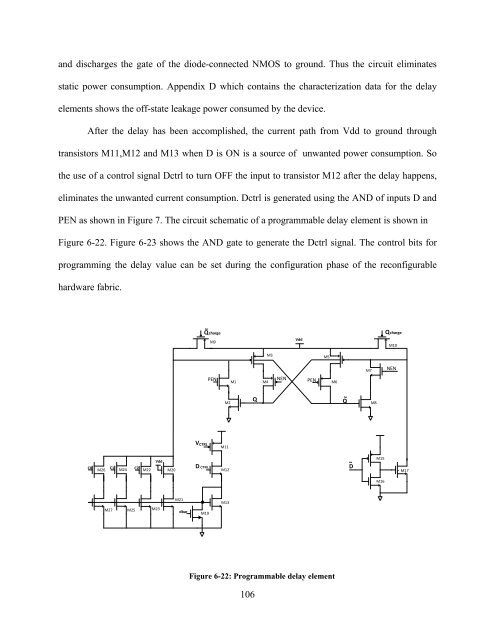
- Page 105 and 106: m-Transistor Cascaded Inverter This
- Page 107 and 108: 6.2 LOW POWER FABRIC USING DELAY EL
- Page 109 and 110: The use of delay elements in the ha
- Page 111 and 112: 6.3.2 Dynamic Triggering Scheme A d
- Page 113 and 114: Figure 6-16 shows the shunt current
- Page 115 and 116: td1 is the delay in discharging nod
- Page 117 and 118: δt is the regeneration time of the
- Page 119 and 120: transistors, they are active low si
- Page 121 and 122: delay elements are enabled on a log
- Page 123: charge sharing happens between the
- Page 127 and 128: uffer with a drive capacity of 640f
- Page 129 and 130: Cell Rise Delay The Cell Rise Delay
- Page 131 and 132: Fall Transition Time The time taken
- Page 133 and 134: 6.5.6 Characterization Results for
- Page 135 and 136: 7.0 EEPROM CIRCUIT DESIGN EEPROM (E
- Page 137 and 138: 7.1.1 Erase Operation Figure 7-3: I
- Page 139 and 140: 7.1.2 Write Operation Figure 7-6: I
- Page 141 and 142: Figure 7-9: IV Characteristics of a
- Page 143 and 144: The current source IFN, resistor RT
- Page 145 and 146: Figure 7-11: HSPICE Description of
- Page 147 and 148: 7.2.1 Ramp Generator The ramp gener
- Page 149 and 150: 7.2.4 Column Latch for Bitlines inp
- Page 151 and 152: 7.2.5 Power Multiplexer Figure 7-16
- Page 153 and 154: The inverter pair connected to the
- Page 155 and 156: 7.2.7 Memory Bank Architecture Figu
- Page 157 and 158: 7.2.8 Memory Bank Simulation Figure
- Page 159 and 160: (Vpp) and a normal voltage (Vdd), t
- Page 161 and 162: 8.1.2 Dynamic Decoder The address d
- Page 163 and 164: 8.3 POWER-ON RESET One problem with
- Page 165 and 166: Figure 8-6 shows the modified charg
- Page 167 and 168: To study the impact of the power co
- Page 169 and 170: 9.0 CONCLUSION For this thesis, I h
- Page 171 and 172: definitions, metal layer resistance
- Page 173 and 174: APPENDIX B element standard cell ch
- Page 175 and 176:
$k=-1; $j=-1; $i=-1; foreach $ load
- Page 177 and 178:
$FALL_START_8 = $OFFSET8 + $ONTIME;
- Page 179 and 180:
if ($#rise_power_6 == -1) { # $modi
- Page 181 and 182:
$modified_spice_array[$i] = $temp2;
- Page 183 and 184:
@fall_power_9 = grep(/fall_power9/,
- Page 185 and 186:
print MEASHANDLE $_; print ENERGYHA
- Page 187 and 188:
} print MEASHANDLE " "; print ENERG
- Page 189 and 190:
set VAL [expr "$NUMBER_OF_MODULES_P
- Page 191 and 192:
set DIE_WIDTH_STRIPE [expr {($MODUL
- Page 193 and 194:
#*************************PLACING i
- Page 195 and 196:
preassignPin stripe $PIN_NAME -loc
- Page 197 and 198:
set X_LOC [expr {($X _LOC -( 31*$OU
- Page 199 and 200:
#Module related details set NUMBER_
- Page 201 and 202:
set X_LOC 0 set Y_LOC 41.2 for {set
- Page 203 and 204:
Table D 1 (Continued) 506.232fF 0.0
- Page 205 and 206:
121.344fF 0.076ns 0.4634 0.2277 570
- Page 207 and 208:
Table D 5 (Continued) 9.48 0. 516 0
- Page 209 and 210:
Table D 7: Characterization data fo
- Page 211 and 212:
Transi tion Table D 9: Characteriza
- Page 213 and 214:
[13] M.F. Aburdene, J. Zheng, and R