- Page 1 and 2:
MCC TECHNICAL REPORT MCC-ECESM-001-
- Page 3 and 4:
MCC Technical Report Document No. M
- Page 5 and 6:
Table of Contents Electronics Indus
- Page 7 and 8:
Electronics Industry Environmental
- Page 9:
Electronics Industry Environmental
- Page 12 and 13:
Electronics Industry Environmental
- Page 15 and 16:
Executive Summary Electronics Indus
- Page 17 and 18:
Electronics Industry Environmental
- Page 19 and 20:
1.0 Introduction Introduction 1.1 O
- Page 21 and 22:
Introduction These kinds of cross-c
- Page 23 and 24:
Introduction Strategic Priority Nee
- Page 25 and 26:
Introduction Tactical Priority Need
- Page 27 and 28:
2.0 Strategic Business Opportunitie
- Page 29 and 30:
Strategic Business Opportunities To
- Page 31 and 32:
Strategic Business Opportunities Go
- Page 33 and 34:
Strategic Business Opportunities co
- Page 35 and 36:
Strategic Business Opportunities Th
- Page 37 and 38:
Strategic Business Opportunities -
- Page 39 and 40:
Environmental Cost Accounting at AT
- Page 41 and 42:
Strategic Business Opportunities Pr
- Page 43 and 44:
Strategic Business Opportunities sm
- Page 45 and 46:
Strategic Business Opportunities pr
- Page 47 and 48:
Strategic Business Opportunities en
- Page 49:
Priority Need Task 1. Knowledge of
- Page 52 and 53:
Information and Knowledge Systems m
- Page 54 and 55:
Information and Knowledge Systems T
- Page 56 and 57:
Information and Knowledge Systems T
- Page 58 and 59:
Information and Knowledge Systems 4
- Page 60 and 61:
Information and Knowledge Systems A
- Page 62 and 63: Information and Knowledge Systems 4
- Page 64 and 65: Information and Knowledge Systems m
- Page 66 and 67: Information and Knowledge Systems 4
- Page 69 and 70: Design for Environment: Evolution a
- Page 71 and 72: Design for Environment: Evolution a
- Page 73 and 74: Design for Environment: Evolution a
- Page 75 and 76: Design for Environment: Evolution a
- Page 77 and 78: Design for Environment: Evolution a
- Page 79 and 80: 5. Models to support more comprehen
- Page 81 and 82: 5.0 Disposition Disposition 5.1 Obj
- Page 83 and 84: Disposition due date are called con
- Page 85 and 86: Disposition 5.4.1 The Consumer/Comm
- Page 87 and 88: Disposition 5.4.2 Recycled Material
- Page 89 and 90: Disposition One of the greatest cha
- Page 91 and 92: Disposition Assistance (OEA) submit
- Page 93 and 94: Disposition provision in other inst
- Page 95 and 96: Disposition The proposals strongly
- Page 97 and 98: 5.5.5 Summary: Lessons from Program
- Page 99 and 100: Disposition The left side of the mo
- Page 101 and 102: Disposition and government for esta
- Page 103 and 104: Disposition Recycling: The collecti
- Page 105: Disposition 87
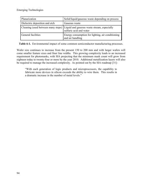
- Page 108 and 109: Emerging Technologies self-aligned
- Page 110 and 111: Emerging Technologies wafer. 18 Gen
- Page 114 and 115: Emerging Technologies Therefore, gi
- Page 116 and 117: Emerging Technologies Printed Wirin
- Page 118 and 119: Emerging Technologies 100 ensures f
- Page 120 and 121: Emerging Technologies Etch Chemical
- Page 122 and 123: Emerging Technologies 104 Fully Sub
- Page 124 and 125: Emerging Technologies adhesives and
- Page 126 and 127: Emerging Technologies 108 have sign
- Page 128 and 129: Emerging Technologies 110 of automa
- Page 130 and 131: Emerging Technologies 112 managemen
- Page 132 and 133: Emerging Technologies 6.4.4 Fully A
- Page 134 and 135: Emerging Technologies 116 Priority
- Page 137 and 138: Appendix A. Other Industry Roadmaps
- Page 139 and 140: Appendix A Overriding Issue SIA/SEM
- Page 141 and 142: Appendix A Integrated Circuit Fabri
- Page 143 and 144: IPC OIDA SIA/SEMATECH Interconnect
- Page 145 and 146: Appendix A IPC Substrate thickness
- Page 147 and 148: SIA/SEMATECH Precision Electromecha
- Page 149 and 150: Appendix A SIA/SEMATECH As CMOS tec
- Page 151 and 152: Appendix A IPC “The coordination
- Page 153 and 154: Appendix A OIDA Specific technical
- Page 155 and 156: Appendix A NEMI Photonics Critical
- Page 157 and 158: Appendix A SIA/SEMATECH In a steady
- Page 159 and 160: Appendix A SIA/SEMATECH Hand-in-han
- Page 161 and 162: Appendix A SIA/SEMATECH Chemical, e
- Page 163 and 164:
Appendix A IPC Several approaches m
- Page 165 and 166:
Appendix A SIA/SEMATECH Conversion
- Page 167 and 168:
SIA/SEMATECH Benchmarking NEMI Need
- Page 169 and 170:
Appendix A IPC Purchasing Suppliers
- Page 171 and 172:
Appendix B. The Ten Ceres Principle
- Page 173 and 174:
Appendix C. The ICC Business Charte
- Page 175 and 176:
Appendix D Appendix D. Statistical
- Page 177 and 178:
SIC CODE Table 1. Demographic and w
- Page 179 and 180:
Appendix D Table 2. Correlation of
- Page 181 and 182:
SIC Code Table 3. Costs of fuels an
- Page 183 and 184:
3672 Printed Circuit Boards 3674 Se
- Page 185 and 186:
1 Value of shipments for product by
- Page 187 and 188:
3676- Electronic resistors 3677- El
- Page 189 and 190:
Appendix D Product Product Company
- Page 191 and 192:
Appendix D Product Product Company
- Page 193 and 194:
Appendix D Product Product Company
- Page 195 and 196:
Appendix D Product Product Company
- Page 197 and 198:
Appendix D Product Product Company
- Page 199 and 200:
Appendix D Product Product Company
- Page 201 and 202:
Appendix D 183
- Page 203 and 204:
Appendix D Table 9. Quantity and va
- Page 205 and 206:
Appendix D Product Product Company
- Page 207 and 208:
Appendix D Product Product Company
- Page 209 and 210:
Key to Table 9: - Represents zero.
- Page 211 and 212:
SIC Code 36 361 Table 10. Air pollu
- Page 213 and 214:
SIC Code 36 361 362 Table 11. Pollu
- Page 215 and 216:
SIC Code 36 Appendix D Table 12. Po
- Page 217 and 218:
Appendix E Appendix E. Development
- Page 219 and 220:
Appendix E releases with component
- Page 221 and 222:
Appendix E 2 1 ITEM: Common Sense I
- Page 223 and 224:
Appendix E 6 1 ITEM: U.S. Industria
- Page 225 and 226:
Appendix E 1 ITEM: Waste Wi$e 2 SOU
- Page 227 and 228:
Appendix E 14 1 ITEM: 33/50 Program
- Page 229 and 230:
Appendix E 3 CONTENT: This Departme
- Page 231 and 232:
Appendix E clearinghouses, database
- Page 233 and 234:
5 COST: Free access to all data/inf
- Page 235 and 236:
Appendix E 34 1 ITEM: EMPF (Electro
- Page 237 and 238:
Appendix E 37 1 ITEM: I3LA (Initiat
- Page 239 and 240:
Appendix E 40 1 ITEM: Access EPA 2
- Page 241 and 242:
Appendix E 7 PERTINENCE: Probably n
- Page 243 and 244:
Appendix E 3 CONTENT: Large indexed
- Page 245 and 246:
Appendix E 55 1 ITEM: UCLA Center f
- Page 247 and 248:
Item # Type Source of Item Access C
- Page 249 and 250:
Appendix F. Survey of Tool Characte
- Page 251 and 252:
[Definitions for the design activit
- Page 253 and 254:
Human Interface (Please rank the im
- Page 255 and 256:
Appendix F 5 Quantifies and reports
- Page 257 and 258:
Appendix G Appendix G. Building Blo
- Page 259 and 260:
Appendix G The Nordic cooperation g
- Page 261:
Appendix G undertaken to assess env
- Page 264 and 265:
Appendix H If no accrual is made be
- Page 266 and 267:
Appendix H 248
- Page 268 and 269:
Appendix I 250
- Page 270 and 271:
Appendix J The ordinance requires U
- Page 272 and 273:
Appendix J 254 150,001 to 600,000 1
- Page 274 and 275:
Appendix J Germany (Proposed; effec
- Page 276 and 277:
References [16] Waitz and Corbet,
- Page 278:
References 260