1996 Electronics Industry Environmental Roadmap - Civil and ...
1996 Electronics Industry Environmental Roadmap - Civil and ...
1996 Electronics Industry Environmental Roadmap - Civil and ...

You also want an ePaper? Increase the reach of your titles
YUMPU automatically turns print PDFs into web optimized ePapers that Google loves.
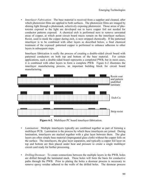
Emerging Technologies<br />
Innerlayer Fabrication: The base material is received from a supplier <strong>and</strong> cleaned, after<br />
which photoresist films are applied to both surfaces. The photoresist films are imaged by<br />
shining light through a photomask, selectively exposing photoresist. Those areas of photoresist<br />
exposed to the light are developed out to leave copper foil not needed for<br />
conductor patterns exposed. A chemical etch is performed next to remove unwanted<br />
areas of copper, at which point circuit board traces remain on the innerlayer surfaces.<br />
Resist, used to mask the copper during etch, is next stripped chemically. If the patterned<br />
innerlayer is to be combined with other layers as described below, a final chemical<br />
treatment of the exposed/ patterned copper is performed to enhance adhesion to other<br />
layers in subsequent steps.<br />
Innerlayer fabrication is really the process of creating a double-sided circuit board with<br />
patterned conductors on both top <strong>and</strong> bottom of the base material. For certain<br />
applications, such a double-sided board represents a completed PWB, but in most cases,<br />
it is combined with other layers to form a complete PWB. Figure 6-2 illustrates the<br />
innerlayer manufacturing process, an important building block for circuit board<br />
manufacturing.<br />
<br />
<br />
<br />
<br />
<br />
<br />
<br />
<br />
<br />
<br />
<br />
<br />
<br />
<br />
<br />
<br />
<br />
<br />
<br />
<br />
<br />
<br />
<br />
<br />
<br />
<br />
<br />
<br />
<br />
<br />
<br />
<br />
<br />
<br />
<br />
Resist coat<br />
<strong>and</strong> pattern<br />
undrilled<br />
laminate<br />
Etch Cu<br />
<br />
<br />
<br />
<br />
<br />
<br />
<br />
<br />
<br />
<br />
<br />
Strip resist<br />
<br />
Figure 6-2. Multilayer PC board innerlayer fabrication.<br />
Lamination: Multiple innerlayers typically are combined together as part of forming a<br />
multilayer PCB. Lamination is the process by which these innerlayers are joined. During<br />
lamination, innerlayers are stacked together with a glue layer between them. The glue<br />
layers are often simply base material (impregnated glass cloth) without the copper foils on<br />
the surface. The innerlayers, the glue layer separators, <strong>and</strong> typically a copper foil layer on<br />
top <strong>and</strong> bottom are then placed under heat <strong>and</strong> pressure to create a single multilayer<br />
circuit card ready for further processing.<br />
Drilling/Desmear: To create connections between the multiple layers in the PWB, holes<br />
are drilled through the laminated stack. These holes will form the basis for conductive<br />
paths through the PWB. Prior to plating the holes a desmear process is necessary to<br />
remove epoxy residue adhered to the walls of the drilled holes. The desmear process<br />
99