- Page 2 and 3:
INTRODUCTION TO NANOTECHNOLOGY Char
- Page 4 and 5:
CONTENTS Preface xi 1 Introduction
- Page 6 and 7:
5.2 Carbon Molecules 103 5.2.1 Natu
- Page 8 and 9:
9.4 Excitons 244 9.5 Single-Electro
- Page 10 and 11:
PREFACE In recent years nanotechnol
- Page 12 and 13:
INTRODUCTION The prefix nano in the
- Page 14 and 15:
INTRODUCTION 3 he recognized the ex
- Page 16 and 17:
1000 (I) a 900 4 800 a 900 I 6 700
- Page 18 and 19:
INTRODUCTION 7 developed before the
- Page 20 and 21:
2.1. STRUCTURE 9 mechanics, the res
- Page 22 and 23:
X T 2.1. STRUCTURE 11 Figure 2.4. C
- Page 24 and 25:
2.1. STRUCTURE 13 Figure 2.6. Thirt
- Page 26 and 27:
Sodium Nanoparticle Na, Magic Numbe
- Page 28 and 29:
2.1. STRUCTURE 17 of the large anio
- Page 30 and 31:
2.1. STRUCTURE 19 other, and high-f
- Page 32 and 33:
2.2. ENERGY BANDS 21 Conduction Ban
- Page 34 and 35:
2.2. ENERGY BANDS 23 Figure 2.13. S
- Page 36 and 37:
2.2. ENERGYBANDS 25 band at point T
- Page 38 and 39:
A X ' Wavevector A Si c z 2.2. ENER
- Page 40 and 41:
2.2. ENERGY BANDS 29 bands of Figs.
- Page 42 and 43:
2.3. LOCALIZED PARTICLES 31 add ele
- Page 44 and 45:
1 meV 10 meV 100 meV FJ E W 1 eV 10
- Page 46 and 47:
3 METHODS OF MEASURING PROPERTIES 3
- Page 48 and 49:
3.2. STRUCTURE 37 Table 3.1. Crysta
- Page 50 and 51:
3.2. STRUCTURE 39 Figure 3.2. Two-d
- Page 52 and 53:
3.2. STRUCTURE 41 The widths of the
- Page 55 and 56:
44 METHODS OF MEASURING PROPERTIES
- Page 57 and 58:
46 METHODS OF MEASURING PROPERTIES
- Page 59 and 60:
48 METHODS OF MEASURING PROPERTIES
- Page 62 and 63:
3.3. MICROSCOPY 51 types of transit
- Page 64 and 65:
3.3. MICROSCOPY 53 Actual diverging
- Page 66 and 67:
Tunneling current Tunneling current
- Page 68 and 69:
3.3. MrCAOSCOPY 57 and the latter m
- Page 70 and 71:
3.4. SPECTROSCOPY 59 From Eq. (3.8)
- Page 72 and 73:
1 Average Panicle FWHM Size (nm) in
- Page 74 and 75:
CdSe colloidal NCs a = 1.2 nrn 3.4.
- Page 76 and 77:
El X-RAY TUBE 8000 - A 6000 - 4000
- Page 78 and 79: 2 N I w 3.0 2.5 2.0 1.5 1 .o 0.5 3.
- Page 80 and 81: i 3.4. SPECTROSCOPY 69 NMR involves
- Page 82 and 83: T=220K - 2G H FURTHER READING 71 Fi
- Page 84 and 85: NUMBER OF ATOMS RADIUS (nm) 1 10 1
- Page 86 and 87: I L 7 3 5 7 9 11 13 15 17 NUMBER OF
- Page 88 and 89: JELLIUM MODEL OF CLUSTERS ATOMS CLU
- Page 90 and 91: 1.02 { 1.01 - 1 - 0.99 - 4.2. METAL
- Page 92 and 93: 4.2. METAL NANOCLUSTERS 81 Figure 4
- Page 94 and 95: 4.2. METAL NANOCLUSTERS 83 Figure 4
- Page 96 and 97: -0 100 200 300 400 500 600 MASSICHA
- Page 98 and 99: a 42. METAL NANOCLUSTERS 87 Figure
- Page 100 and 101: . . . .. . - . D 111111111111111111
- Page 102 and 103: 3 4 2.5 0 cn g 2 0 z d 1.5 t a 9 1
- Page 104 and 105: 4.3. SEMICONDUCTING NANOPARTICLES 9
- Page 106 and 107: 4.4. RARE GAS AND MOLECULAR CLUSTER
- Page 108 and 109: 4.5. METHODS OF SYNTHESIS 97 d Figu
- Page 110 and 111: 4.5. METHODS OF SYNTHESIS 99 isopro
- Page 112 and 113: PULSED LASER BEAM 1 1 1 1 1 I ROTAT
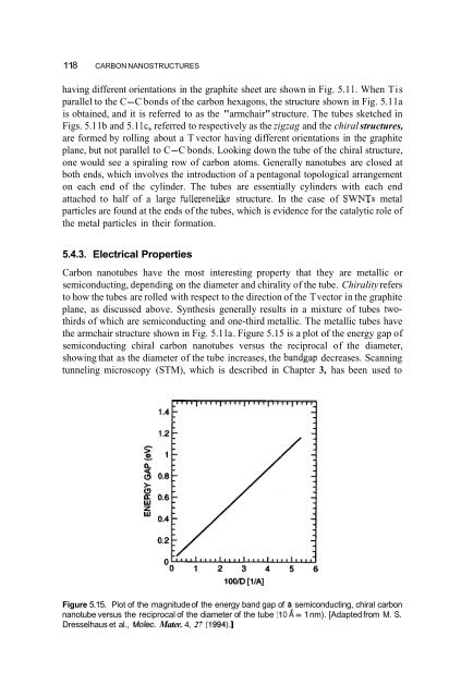
- Page 114 and 115: 5.1. INTRODUCTION CARBON NANOSTRUCT
- Page 116 and 117: 5.2. CARBON MOLECULES 105 methane d
- Page 118 and 119: 5.3. CARBON CLUSTERS 107 -0 20 40 6
- Page 120 and 121: PHOTON ENERGY (electron volts) 5.3.
- Page 122 and 123: Figure 5.6. Structure of the CEO fu
- Page 124 and 125: 1 30 0 14.1 14.2 14.3 14.4 14.5 LAT
- Page 126 and 127: (c) 5.4. CARBON NANOTUBES 115 Figur
- Page 130 and 131: 5.4. CARBON NANOTUBES 11 9 investig
- Page 132 and 133: 5.4. CARBON NANOTUBES 121 energy gr
- Page 134 and 135: 5.4. CARBON NANOTUBES 123 stretch c
- Page 136 and 137: 5.5. APPLICATIONS OF CARBON NANOTUB
- Page 138 and 139: 5.5. APPLICATIONS OF CARBON NANOTUB
- Page 140 and 141: - v) 450 : 400 3 350 1 300 : 5 250
- Page 142 and 143: 5.5. APPLICATIONS OF CARBON NANOTUB
- Page 144 and 145: BULK NANOSTRUCTURED MATERIALS In th
- Page 146 and 147: h 8 0 6.1. SOLID DISORDERED NANOSTR
- Page 148 and 149: 6.1. SOLID DISORDERED NANOSTRUCTURE
- Page 150 and 151: 6.1. SOLID DISORDERED NANOSTRUCTURE
- Page 152 and 153: 6.1. SOLID DISORDERED NANOSTRUCTURE
- Page 154 and 155: 6.1. SOLID DISORDERED NANOSTRUCTURE
- Page 156 and 157: 6.1. SOLID DISORDERED NANOSTRUCTURE
- Page 158 and 159: 6.1. SOLID DISORDERED NANOSTRUCTURE
- Page 160 and 161: 6.1. SOLID DISORDERED NANOSTRUCTURE
- Page 162 and 163: 6.1. SOLID DISORDERED NANOSTRUCTURE
- Page 164 and 165: 6.2. NANOSTRUCTURED CRYSTALS 153 qu
- Page 166: 6.2. NANOSTRUCTURED CRYSTALS 155 Fi
- Page 169 and 170: 158 BULK NANOSTRUCTURED MATERIALS 6
- Page 171 and 172: 160 BULK NANOSTRUCTURED MATERIALS w
- Page 173 and 174: 162 BULK NANOSTRUCTURED MATERIALS 0
- Page 175 and 176: 164 BULK NANOSTRUCTURED MATERIALS n
- Page 177 and 178: 166 NANOSTRUCTURED FERROMAGNETISM f
- Page 179 and 180:
168 NANOSTRUCTURED FERROMAGNETISM i
- Page 181 and 182:
170 NANOSTRUCTURED FERROMAGNETISM M
- Page 183 and 184:
172 NANOSTRUCTURED FERROMAGNETISM h
- Page 185 and 186:
174 NANOSTRUCTURED FERROMAGNETISM d
- Page 187 and 188:
176 NANOSTRUCTURED FERROMAGNETISM o
- Page 190 and 191:
4 h $ 3 7.5. NANOCARBON FERROMAGNET
- Page 192 and 193:
7.6. GIANT AND COLOSSAL MAGNETORESI
- Page 194 and 195:
1.4 N 1 1.2 z " 1 0 v 5 h 0.8 0 0.6
- Page 196 and 197:
7.6. GIANT AND COLOSSAL MAGNETORESI
- Page 198 and 199:
7.7. FERROFLUIDS 187 Figure 7.22. M
- Page 200 and 201:
7.7. FECIROFLUIDS 189 Figure 7.25.
- Page 202 and 203:
7.7. FERRQFLUlOS 191 FerroRuids can
- Page 204 and 205:
FURTHER READING FURTHER READING 193
- Page 206 and 207:
10- IR f IA -1 8.1. INTRODUCTION 19
- Page 208 and 209:
8.2. INFRARED FREQUENCY RANGE 197 1
- Page 210 and 211:
8.2. INFRARED FREQUENCY RANGE 199 d
- Page 212 and 213:
s C CTI e 8 9 4( 8.2. INFRARED FREQ
- Page 214 and 215:
8.2.3. Raman Spectroscopy 8.2. INFR
- Page 216 and 217:
8.2. INFRARED FREQUENCY RANGE 205 a
- Page 218 and 219:
- r I 520 51 8 v 6 516 a" 51 4 51 2
- Page 220 and 221:
8.2. INFRARED FREQUENCY RANGE 209 i
- Page 222 and 223:
v) - C 3 8 600 400 100 0 e e 10 20
- Page 224 and 225:
i E (cm-’ ) 20 c I 1 ID 0 4x10⁷ 8
- Page 226 and 227:
- ? m v .- - z In C a, c C - .. . .
- Page 228 and 229:
Excitatior I [eV]: 2.175 2.214 2.25
- Page 230 and 231:
6 100 200 300 Time (ns) 8.3. LUMINE
- Page 232 and 233:
400 nm Laser / Free excitons Trappe
- Page 234 and 235:
8.4. NANOSTRUCTURES IN ZEOLITE CAGE
- Page 236 and 237:
FURTHER READING 225 P. Milani and C
- Page 238 and 239:
9.2. PREPARATION OF QUANTUM NANOSTR
- Page 240 and 241:
i 9.2. PREPARATION OF QUANTUM NANOS
- Page 242 and 243:
9.3. SIZE AND DIMENSIONALITY EFFECT
- Page 244 and 245:
9.3. SIZE AND DIMENSIONALITY EFFECT
- Page 246 and 247:
9.3. SIZE AND DIMENSIONALITY EFFECT
- Page 248 and 249:
w n 3 2 1 9.3. SIZE AND DIMENSIONAL
- Page 250 and 251:
9.3. SIZE AND DIMENSIONALITY EFFECT
- Page 252 and 253:
9.3. SIZE AND DIMENSIONALITY EFFECT
- Page 254 and 255:
WE) Quantum Dot Number of Electrons
- Page 256 and 257:
9.5. SINGLE-ELECTRON TUNNELING 245
- Page 258 and 259:
9.5. SINGLE-ELECTRON TUNNELING 247
- Page 260 and 261:
1 pair section ;- COT. .; . . I. .
- Page 262 and 263:
o.6 LWIR: T = 77 K 45" incidence AD
- Page 264 and 265:
9.7. SUPERCONDUCTIVITY 253 horizont
- Page 266 and 267:
9.7. SUPERCONDUCTIVITY 255 applied
- Page 268 and 269:
10.1. SELF-ASSEMBLY 10 SELF-ASSEMBL
- Page 270 and 271:
10.1. SELF-ASSEMBLY 259 factor of 2
- Page 272 and 273:
(a) (LI (dl 10.1. SELF-ASSEMBLY 261
- Page 274 and 275:
10.1. SELF-ASSEMBLY 263 atoms, as n
- Page 276 and 277:
- c v) ._ C 3 2 9 40 c - .- e m v w
- Page 278 and 279:
10.2. CATALYSIS 267 where the lengt
- Page 280 and 281:
10.2. CATALYSIS 269 are also other
- Page 282 and 283:
1600 2 1200 t p - Bi2M020, 10.2. CA
- Page 284 and 285:
7 - I 2,330 m .- c r 0 2 2,300 - u)
- Page 286 and 287:
10.2. CATALYSIS 275 with a top and
- Page 288 and 289:
10.2. CATALYSIS 277 based on the pr
- Page 290 and 291:
10.2. CATALYSIS 279 CnHlnfl, which
- Page 292 and 293:
I1 ORGANIC COMPOUNDS AND POLYMERS 1
- Page 294 and 295:
11.2. FORMING AND CHARACTERIZING PO
- Page 296 and 297:
1 1.3. NANOCRYSTALS 285 This expres
- Page 298 and 299:
-1 5 0) C a, -1 1 000 300 100 30 10
- Page 300 and 301:
11.3. NANOCRYSTALS 289 Table 11.1.
- Page 302 and 303:
11.3. NANOCRYSTALS 291 R’ groups
- Page 304 and 305:
11.4. POLYMERS 293 Figure 11.9. Ske
- Page 306 and 307:
11.5. SUPRAMOLECULAR STRUCTURES 295
- Page 308 and 309:
M Et3P OTf M=Pd M=Pt M=Pd, 41 % M=P
- Page 310 and 311:
11.5. SVPRAMOLECUUAR STRUCTURES 2s
- Page 312 and 313:
11.5. SUPRAMOLECULAR STRUCTURES 301
- Page 314 and 315:
11 5. SUPRAMOLECULAR STRUCTURES 303
- Page 316 and 317:
11.5. SUPRAMOLECULAR STRUCTURES 305
- Page 318 and 319:
BiodegradaWe surface 4 Functional g
- Page 320 and 321:
FURTHER READING 309 F. J. Owens and
- Page 322 and 323:
12.2. BIOLOGICAL BUILDING BLOCKS 31
- Page 325 and 326:
314 BIOLOGICAL MATERIALS which we w
- Page 327 and 328:
316 BIOLOGICAL MATERIALS Table 12.2
- Page 329 and 330:
318 BIOLOGICAL MATERtALS i J / Flgu
- Page 331 and 332:
320 BIOLOGICAL MATERIALS Pyrimidine
- Page 333 and 334:
322 BlOLMjlCAL MATERiALS (a) DNA do
- Page 335 and 336:
324 BIOLOGICAL MATERIALS so each wo
- Page 337 and 338:
326 BIOLOGICAL MATERIALS 12.4.2. Mi
- Page 339 and 340:
328 BIOLOGICAL MATERIALS tions they
- Page 341 and 342:
330 BIOLOGICAL MATERIALS hardened f
- Page 343 and 344:
13 NANOMACHINES AND NANODEVICES In
- Page 345 and 346:
334 NANOMACHINES AND NANODEVICES CA
- Page 347 and 348:
336 NANOMACHINES AND NANODEVICES Op
- Page 349 and 350:
338 NANOMACHINES AND NANODEVICES ti
- Page 351 and 352:
340 NANOMACHINES AN0 NANODEVICES PO
- Page 353 and 354:
342 NANOMACHINES AND NANODEVICES X
- Page 355 and 356:
344 NANOMACHINES AND NANODEVICES na
- Page 357 and 358:
346 NANOMACHINES AND NANODEVICES 31
- Page 359 and 360:
348 NANOMACHINES AND NANODEVICES -
- Page 361 and 362:
350 NANOMACHINES AND NANODEVICES re
- Page 363 and 364:
352 NANOMACHINES AND NANODEVICES 1
- Page 365 and 366:
354 NANOMACHINES AND NANODEVICES -1
- Page 368 and 369:
A.l. INTRODUCTION APPENDIX A FORMUL
- Page 370 and 371:
A.3. PARTIAL CONFINEMENT 359 limiti
- Page 372 and 373:
APPENDIX B TABULATIONS OF SEMICONDU
- Page 374 and 375:
TABULATIONS OF SEMICONDUCTING MATER
- Page 376 and 377:
Table B.8. Effective masses m+ rela
- Page 378 and 379:
TABULATIONS OF SEMICONDUCTING MATER
- Page 380:
TABULATIONS OF SEMICONDUCTING MATER
- Page 383 and 384:
372 INDEX amoeba, 3 16 amphiphilic,
- Page 385 and 386:
374 INDEX CdS, 9, 130, 213, 216, 36
- Page 387 and 388:
376 INDEX dispersion, 277 disulfide
- Page 389 and 390:
378 INDEX Ga (gallium) (continued)
- Page 391 and 392:
380 INDEX length (continued) critic
- Page 393 and 394:
382 INDEX multiple ionization, 93 r
- Page 395 and 396:
384 INDEX pi-conjugation, 282, 292
- Page 397 and 398:
silica, 269 silica-alumina, 269, 27
- Page 399:
388 INDEX wavefimction (continued)